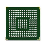
STM32F417IGH6 STMicroelectronics, STM32F417IGH6 Datasheet - Page 109

STM32F417IGH6
Manufacturer Part Number
STM32F417IGH6
Description
Microcontrollers (MCU) ARM M4 1024 FLASH 168 Mhz 192kB SRAM
Manufacturer
STMicroelectronics
Specifications of STM32F417IGH6
Core
ARM Cortex M4
Processor Series
STM32F4
Data Bus Width
32 bit
Maximum Clock Frequency
168 MHz
Program Memory Size
1024 KB
Data Ram Size
192 KB
On-chip Adc
Yes
Number Of Programmable I/os
140
Number Of Timers
10
Operating Supply Voltage
1.7 V to 3.6 V
Package / Case
UFBGA-176
Mounting Style
SMD/SMT
A/d Bit Size
12 bit
A/d Channels Available
24
Interface Type
CAN, I2C, I2S, SPI, UART
Program Memory Type
Flash
Lead Free Status / Rohs Status
Details
Available stocks
Company
Part Number
Manufacturer
Quantity
Price
Company:
Part Number:
STM32F417IGH6
Manufacturer:
STMicroelectronics
Quantity:
480
STM32F415xx, STM32F417xx
5.3.20
Table 64.
R
V
Symbol
C
f
R
ADC
TRIG
V
REF+
t
t
f
V
ADC
latr
AIN
lat
ADC
DDA
AIN
(5)
(5)(7)
(5)
(5)
(5)
(5)
(3)
Power supply
Positive reference voltage
ADC clock frequency
External trigger frequency
Conversion voltage range
External input impedance
Sampling switch resistance
Internal sample and hold
capacitor
Injection trigger conversion
latency
Regular trigger conversion latency
Table 63.
1. TBD stands for “to be defined”.
CAN (controller area network) interface
Refer to
function characteristics (CANTX and CANRX).
12-bit ADC characteristics
Unless otherwise specified, the parameters given in
performed under the ambient temperature, f
conditions summarized in
ADC characteristics
Symbol
t
t
t
su(RXD)
d(TXEN)
t
t
t
ih(RXD)
t
t
su(ER)
d(TXD)
su(DV)
ih(ER)
ih(DV)
Section 5.3.16: I/O port characteristics
Parameter
Dynamics characteristics: Ethernet MAC signals for MII
Receive data setup time
Receive data hold time
Data valid setup time
Data valid hold time
Error setup time
Error hold time
Transmit enable valid delay time
Transmit data valid delay time
(6)
(1)
Table
Rating
Doc ID 022063 Rev 1
V
V
DDA
See
10.
DDA
f
f
f
ADC
ADC
ADC
Conditions
= 1.8
Equation 1
= 2.4 to 3.6 V
details
= 36 MHz
= 36 MHz
= 36 MHz
(2)
to 2.4 V
PCLK2
for
for more details on the input/output alternate
frequency and V
0 (V
tied to ground)
Table 64
TBD
TBD
TBD
TBD
TBD
TBD
13.4
12.9
Min
SSA
1.8
1.8
Min
1.5
0.6
0.6
(2)(4)
4
-
-
or V
-
-
-
-
-
(2)
are derived from tests
REF-
TBD
TBD
TBD
TBD
TBD
TBD
15.5
16.1
Typ
Electrical characteristics
DDA
Typ
-
-
-
-
-
-
-
-
-
-
-
-
-
-
supply voltage
(1)
Max
TBD
TBD
TBD
TBD
TBD
TBD
17.7
19.4
V
0.100
0.067
V
TBD
TBD
TBD
TBD
Max
3
2
3.6
REF+
17
50
DDA
6
(8)
(8)
109/156
Unit
1/f
1/f
1/f
MHz
MHz
ns
ns
ns
ns
ns
ns
ns
ns
Unit
kHz
kΩ
kΩ
pF
µs
µs
V
V
V
ADC
ADC
ADC


