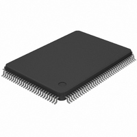
MAX4356ECD+T Maxim Integrated Products, MAX4356ECD+T Datasheet - Page 35

MAX4356ECD+T
Manufacturer Part Number
MAX4356ECD+T
Description
IC VIDEO CROSSPOINT SWIT 128TQFP
Manufacturer
Maxim Integrated Products
Datasheet
1.MAX4356ECD.pdf
(41 pages)
Specifications of MAX4356ECD+T
Function
Video Crosspoint Switch
Circuit
1 x 16:16
Voltage Supply Source
Single, Dual Supply
Voltage - Supply, Single/dual (±)
5V, ± 3 V ~ 5 V
Operating Temperature
-40°C ~ 85°C
Mounting Type
Surface Mount
Package / Case
128-TQFP, 128-VQFP
Lead Free Status / RoHS Status
Lead free / RoHS Compliant
stream equal to n x 96 bits, where n is the number of
MAX4356 devices on the bus. The first 96-bit data word
programs the last MAX4356 in line (see Matrix
Programming under Applications Information).
The MAX4356 features an asynchronous dedicated 2:1
Mux for each output buffer amplifier. Fast 40ns switch-
ing times enable pixel switching for on-screen-display
(OSD) information such as text or other picture-in-pic-
ture signals (Figure 1). OSDFILL_ inputs are buffered
analog inputs connected to each dedicated OSD Mux.
Switching between the programmed IN_ input from the
crosspoint switch matrix and the OSDFILL_ is accom-
plished by driving the dedicated OSDKEY_ digital
input. A logic low on OSDKEY
at OSDFILL
trol does not affect the crosspoint switch matrix pro-
gramming or the output buffer enable/disable or
gain-set programming.
The MAX4356 features an asynchronous bidirectional
RESET with an internal 20k
When RESET is pulled low, either by internal circuitry,
or driven externally, the analog output buffers are
latched into a high-impedance state. After RESET is
released, the output buffers remain disabled. The out-
puts may be enabled by sending a new 96-bit data
word or a 16-bit individual output address word. A reset
is initiated from any of three sources. RESET can be
driven low by external circuitry to initiate a reset, or
RESET can be pulled low by internal circuitry during
power-up (power-on reset) or thermal shutdown.
Since driving RESET low only clears the output buffer
enable bit in the matrix control latches, RESET can be
used to disable all outputs simultaneously. If no new
data has been loaded into the 96-bit complete matrix
mode register, a single UPDATE restores the previous
matrix control settings.
The power-on reset ensures all output buffers are in a
disabled state when power is initially applied. A V
voltage comparator generates the power-on-reset.
When the voltage at V
on-reset comparator pulls RESET low through internal
circuitry. As the digital supply voltage ramps up cross-
ing 2.5V, the MAX4356 holds RESET low for 40ns (typ).
Connecting a small capacitor from RESET to DGND
extends the power-on-reset delay. See Power-on Reset
vs. RESET Capacitance in the Typical Operating
Characteristics.
with On-Screen Display Insertion and I/O Buffers
16 x 16 Nonblocking Video Crosspoint Switch
i
to the OUT
______________________________________________________________________________________
On-Screen-Display Fast Mux
DD
i
output buffer. OSDKEY_ con-
is less than 2.5V, the power-
i
routes the analog signal
pullup resistor to V
Power-On-Reset
RESET
DD
DD
.
The MAX4356 features thermal shutdown protection
with temperature hysteresis. When the die temperature
exceeds +150°C, the MAX4356 pulls RESET low, dis-
abling the output buffers. When the die cools by 20°C,
the RESET pulldown is deasserted, and output buffers
remain disabled until the device is programmed again.
The MAX4356 can be easily used to create larger
switching matrices. The number of ICs required to
implement the matrix is a function of the number of
input channels, the number of outputs required, and
whether the array needs to be nonblocking or not. The
most straightforward technique for implementing non-
blocking matrices is to arrange the building blocks in a
grid. The inputs connect to each vertical bank of
devices in parallel with the other banks. The outputs of
each building block in a vertical column connect
together in a wired-OR configuration. Figure 6 shows a
128-input, 32-output, nonblocking array using the
MAX4356 16 x 16 crosspoint devices.
The wired-OR connection of the outputs shown in the
diagram is possible because the outputs of the IC
devices can be placed in a disabled or high-imped-
ance output state. This disable state of the output
buffers is designed for a maximum impedance vs. fre-
quency while maintaining a low output capacitance.
These characteristics minimize the adverse loading
effects from the disabled outputs. Larger arrays are
constructed by extending this connection technique to
more devices.
Figure 6 shows an implementation requiring many out-
puts to be wired together. This creates a situation
where each output buffer sees not only the normal load
impedance, but also the disabled impedance of all the
other outputs. This impedance has a resistive and a
capacitive component. The resistive components
reduce the total effective load for the driving output.
Total capacitance is the sum of the capacitance of all
the disabled outputs and is a function of the size of the
matrix. Also, as the size of the matrix increases, the
length of the PC board traces increases, adding more
capacitance. The output buffers have been designed to
drive more than 30pF of capacitance while still main-
taining a good AC response. Depending on the size of
the array, the capacitance seen by the output can
exceed this amount. There are several ways to improve
the situation. The first is to use more building-block
Building Large Video Switching Systems
Applications Information
Driving a Capacitive Load
Thermal Shutdown
35


