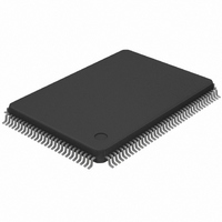
MAX4356ECD+T Maxim Integrated Products, MAX4356ECD+T Datasheet - Page 28

MAX4356ECD+T
Manufacturer Part Number
MAX4356ECD+T
Description
IC VIDEO CROSSPOINT SWIT 128TQFP
Manufacturer
Maxim Integrated Products
Datasheet
1.MAX4356ECD.pdf
(41 pages)
Specifications of MAX4356ECD+T
Function
Video Crosspoint Switch
Circuit
1 x 16:16
Voltage Supply Source
Single, Dual Supply
Voltage - Supply, Single/dual (±)
5V, ± 3 V ~ 5 V
Operating Temperature
-40°C ~ 85°C
Mounting Type
Surface Mount
Package / Case
128-TQFP, 128-VQFP
Lead Free Status / RoHS Status
Lead free / RoHS Compliant
16 x 16 Nonblocking Video Crosspoint Switch
with On-Screen Display Insertion and I/O Buffers
28
15, 17, 19, 21, 23,
16, 18, 20, 65, 66,
29, 67, 71, 75, 79,
68, 70, 72, 74, 76,
78, 80, 82, 84, 86,
88, 90, 92, 94, 96,
69, 73, 77, 81, 85,
83, 87, 91, 95, 99
25, 27, 121, 123,
1–4, 30–38, 103
6, 8, 10, 12, 14,
5, 7, 9, 11, 13,
89, 93, 97, 128
100, 101, 102,
120, 122, 124,
22, 24, 26, 28
______________________________________________________________________________________
125, 127
104–119
49–64
PIN
126
39
40
41
42
43
44
45
46
47
48
98
OSDKEY0–
OSDKEY15
OSDFILL0–
OSDFILL15
IN0–IN15
UPDATE
OUT0–
OUT15
RESET
NAME
AGND
A3–A0
DGND
MODE
DOUT
AOUT
SCLK
N.C.
V
V
DIN
V
CE
CC
DD
EE
No Connection. Not internally connected. Connect to AGND.
Buffered Analog Inputs
Analog Ground
Address Programming Inputs. Connect to DGND or V
output address mode. See Table 3.
Positive Analog Supply. Bypass each pin with a 0.1 F capacitor to AGND. Connect a single
10 F capacitor from one V
Serial Data Output. In complete matrix mode, data is clocked through the 96-bit Matrix Control
Shift register. In individual output address mode, data at DIN passes directly to DOUT.
Digital Ground
Address Recognition Output. AOUT drives low after successful chip address recognition.
Serial Clock Input
Clock Enable Input. Drive low to enable the serial data interface.
Serial Interface Mode Select Input. Drive high for complete matrix mode (mode 1), or drive low
for individual output address mode (mode 0).
Asynchronous Reset Input/Output. Drive RESET low to initiate hardware reset. All matrix
settings are set to power-up defaults and all analog outputs are disabled. Additional power-on
reset delay may be set by connecting a small capacitor from RESET to DGND.
Update Input. Drive UPDATE low to transfer data from Mode registers to the matrix switch.
Serial Data Input. Data is clocked in on the falling edge of SCLK.
Digital Logic Supply. Bypass V
Digital Control Input. Control for the fast 2:1 OSD insertion multiplexer routing signal to output
buffers. A logic high routes the programmed IN_ analog input signal to the output buffer. A
logic low routes the dedicated OSDFILL_ input to the corresponding output buffer.
Buffered Analog Outputs. Gain is individually programmable for A
through the serial interface. Outputs may be individually disabled (high impedance). On
power-up or assertion of RESET, all outputs are disabled.
Negative Analog Supply. Bypass each pin with a 0.1 F capacitor to AGND. Connect a single
10 F capacitor from one V
Dedicated OSD Analog Signal Buffered Inputs. For each output buffer amplifier OSDFILL, the
input signal is routed to output buffer amplifier OUT when the corresponding OSDKEY is low.
CC
EE
pin to AGND.
pin to AGND.
DD
with a 0.1 F capacitor DGND.
FUNCTION
DD
to select the address for individual
V
= +1V/V or A
Pin Description
V
= +2V/V


