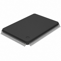
MAX4356ECD+T Maxim Integrated Products, MAX4356ECD+T Datasheet - Page 2

MAX4356ECD+T
Manufacturer Part Number
MAX4356ECD+T
Description
IC VIDEO CROSSPOINT SWIT 128TQFP
Manufacturer
Maxim Integrated Products
Datasheet
1.MAX4356ECD.pdf
(41 pages)
Specifications of MAX4356ECD+T
Function
Video Crosspoint Switch
Circuit
1 x 16:16
Voltage Supply Source
Single, Dual Supply
Voltage - Supply, Single/dual (±)
5V, ± 3 V ~ 5 V
Operating Temperature
-40°C ~ 85°C
Mounting Type
Surface Mount
Package / Case
128-TQFP, 128-VQFP
Lead Free Status / RoHS Status
Lead free / RoHS Compliant
16 x 16 Nonblocking Video Crosspoint Switch
with On-Screen Display Insertion and I/O Buffers
ABSOLUTE MAXIMUM RATINGS
Analog Supply Voltage (V
Digital Supply Voltage (V
Analog Supplies to Analog Ground
Analog Ground to Digital Ground .........................-0.3V to +0.3V
IN_, OSDFILL_ Voltage Range........ (V
OUT_ Short-Circuit Duration to AGND, V
SCLK, CE, UPDATE, MODE, A_, DIN, DOUT,
Stresses beyond those listed under “Absolute Maximum Ratings” may cause permanent damage to the device. These are stress ratings only, and functional
operation of the device at these or any other conditions beyond those indicated in the operational sections of the specifications is not implied. Exposure to
absolute maximum rating conditions for extended periods may affect device reliability.
DC ELECTRICAL CHARACTERISTICS—DUAL SUPPLIES ±5V
(V
unless otherwise noted. Typical values are at T
2
Operating Supply Voltage
Range
Logic Supply Voltage Range
Gain (Note 1)
Gain Matching
(Channel to Channel)
CC
(V
RESET, AOUT, OSDKEY_.......(V
_______________________________________________________________________________________
CC
= +5V, V
- AGND) and (AGND - V
PARAMETER
EE
= -5V, V
DD
CC
DD
- DGND) ...................................+6V
- V
= +5V, AGND = DGND = 0, V
EE
EE
) .....................................+11V
) ......................................+6V
DD
SYMBOL
V
DGND
CC
V
+ 0.3V) to (DGND - 0.3V)
V
DD
A
CC
CC
EE
V
+ 0.3V) to (V
to
, or V
-
A
EE
Guaranteed by PSRR test
(V
A
(V
A
(V
A
(V
A
(V
A
R
R
= +25°C.)
V
V
V
V
V
L
L
......Indefinite
EE
EE
EE
EE
EE
= 10k
= 150
= +1V/V, R
= +1V/V, R
= +2V/V, R
= +2V/V, R
= +1V/V, R
+ 2.5V) < V
+ 2.5V) < V
+ 3.75V) < V
+ 3.75V) < V
+ 1V) < V
EE
- 0.3V)
IN
L
L
L
L
L
IN
CONDITIONS
_= 0, V
= 150
= 10k
= 150
= 10k
= 10k
IN
IN
_
< (V
IN
IN
_
_
< (V
< (V
_
_
< (V
< (V
Current into Any Analog Input Pin (IN_, OSDFILL_) .........±50mA
Current into Any Analog Output Pin (OUT_).....................±75mA
Continuous Power Dissipation (T
Operating Temperature Range ...........................-40°C to +85°C
Junction Temperature ......................................................+150°C
Storage Temperature Range .............................-65°C to +150°C
Lead Temperature (soldering, 10s) ................................ +300°C
CC
OSDFILL
CC
CC
128-Pin TQFP (derate 25mW/°C above +70°C).................2W
CC
CC
- 1.2V),
- 2.5V),
- 2.5V),
- 3.75V),
- 3.75V)
_ = 0, R
L
= 150
0.97
0.99
1.92
1.94
0.95
MIN
4.5
2.7
to AGND, and T
A
= +70°C)
0.995
0.999
1.996
2.008
0.994
TYP
0.5
0.5
A
MAX
= T
10.5
2.08
2.06
5.5
1.5
1
1
1
2
MIN
to T
UNITS
V/V
%
V
V
MAX
,


