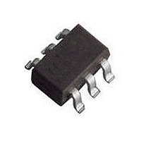
74LVC2G17GW-G NXP Semiconductors, 74LVC2G17GW-G Datasheet - Page 4

74LVC2G17GW-G
Manufacturer Part Number
74LVC2G17GW-G
Description
Buffers & Line Drivers 3.3V DUAL SCHMITT TRIGGER BUFF
Manufacturer
NXP Semiconductors
Datasheet
1.74LVC2G17GV125.pdf
(19 pages)
Specifications of 74LVC2G17GW-G
Logic Family
LVC
Logic Type
CMOS
Number Of Channels Per Chip
2
Polarity
Non-Inverting
Supply Voltage (max)
5.5 V
Supply Voltage (min)
1.65 V
Maximum Operating Temperature
+ 125 C
Mounting Style
SMD/SMT
Package / Case
SOT-363-6
High Level Output Current
- 32 mA
Low Level Output Current
32 mA
Minimum Operating Temperature
- 40 C
Number Of Lines (input / Output)
2 / 2
Propagation Delay Time
3.8 ns at 2.7 V
Lead Free Status / Rohs Status
Details
Other names
74LVC2G17GW,125
NXP Semiconductors
9. Limiting values
Table 5.
In accordance with the Absolute Maximum Rating System (IEC 60134). Voltages are referenced to GND (ground = 0 V).
[1]
[2]
[3]
10. Recommended operating conditions
Table 6.
11. Static characteristics
Table 7.
At recommended operating conditions; voltages are referenced to GND (ground = 0 V).
74LVC2G17
Product data sheet
Symbol
V
I
V
I
V
I
I
I
T
P
Symbol
V
V
V
T
Symbol Parameter
T
V
IK
OK
O
CC
GND
stg
amb
amb
CC
I
O
tot
CC
I
O
OL
The input and output voltage ratings may be exceeded if the input and output current ratings are observed.
When V
For SC-88 and SC-74 packages: above 87.5 °C the value of P
For XSON6 packages: above 118 °C the value of P
= −40 °C to +85 °C
LOW-level output voltage
CC
Limiting values
Recommended operating conditions
Static characteristics
= 0 V (Power-down mode), the output voltage can be 5.5 V in normal operation.
Parameter
supply voltage
input clamping current
input voltage
output clamping current
output voltage
output current
supply current
ground current
storage temperature
total power dissipation
Parameter
supply voltage
input voltage
output voltage
ambient temperature
[1]
Conditions
V
I
All information provided in this document is subject to legal disclaimers.
I
I
I
I
I
I
= V
O
O
O
O
O
O
= 100 μA; V
= 4 mA; V
= 8 mA; V
= 12 mA; V
= 24 mA; V
= 32 mA; V
CC
Active mode
Conditions
V
V
Power-down mode
V
T
Conditions
or GND
tot
amb
I
O
O
Rev. 5 — 6 August 2010
< 0 V
derates linearly with 7.8 mW/K.
< 0 V
= 0 V to V
= −40 °C to +125 °C
CC
CC
Dual non-inverting Schmitt trigger with 5 V tolerant input
CC
CC
CC
CC
= 1.65 V
= 2.3 V
tot
= 2.7 V
= 3.0 V
= 4.5 V
= 1.65 V to 5.5 V
derates linearly with 4.0 mW/K.
CC
Min
-
-
-
-
-
-
[1][2]
[1][2]
[1]
[3]
Min
1.65
0
0
−40
Min
−0.5
-
−0.5
-
−0.5
−0.5
-
-
-
−65
-
74LVC2G17
Typ
-
-
-
-
-
-
Typ
-
-
-
-
Max
+6.5
−50
+6.5
−50
V
+6.5
±50
100
−100
+150
300
CC
© NXP B.V. 2010. All rights reserved.
+ 0.5
Max
0.1
0.45
0.3
0.4
0.55
0.55
Max
5.5
5.5
V
+125
CC
Unit
V
mA
V
mA
V
V
mA
mA
mA
°C
mW
Unit
V
V
V
°C
Unit
V
V
V
V
V
V
4 of 19


