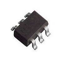
74LVC2G17GW-G NXP Semiconductors, 74LVC2G17GW-G Datasheet - Page 15

74LVC2G17GW-G
Manufacturer Part Number
74LVC2G17GW-G
Description
Buffers & Line Drivers 3.3V DUAL SCHMITT TRIGGER BUFF
Manufacturer
NXP Semiconductors
Datasheet
1.74LVC2G17GV125.pdf
(19 pages)
Specifications of 74LVC2G17GW-G
Logic Family
LVC
Logic Type
CMOS
Number Of Channels Per Chip
2
Polarity
Non-Inverting
Supply Voltage (max)
5.5 V
Supply Voltage (min)
1.65 V
Maximum Operating Temperature
+ 125 C
Mounting Style
SMD/SMT
Package / Case
SOT-363-6
High Level Output Current
- 32 mA
Low Level Output Current
32 mA
Minimum Operating Temperature
- 40 C
Number Of Lines (input / Output)
2 / 2
Propagation Delay Time
3.8 ns at 2.7 V
Lead Free Status / Rohs Status
Details
Other names
74LVC2G17GW,125
NXP Semiconductors
Fig 18. Package outline SOT1202 (XSON6)
74LVC2G17
Product data sheet
XSON6: extremely thin small outline package; no leads;
6 terminals; body 1.0 x 1.0 x 0.35 mm
Dimensions
Note
1. Including plating thickness.
2. Visible depending upon used manufacturing technology.
mm
SOT1202
Unit
Outline
version
max
nom
min
0.35 0.04
A
(1)
A
1
0.20
0.15
0.12
b
IEC
terminal 1
index area
1.05
1.00
0.95
e
D
(6×)
L
(2)
1.05
1.00
0.95
1
E
0.55 0.35
JEDEC
e
1
6
All information provided in this document is subject to legal disclaimers.
e
e
1
1
References
D
2
5
0.35
0.30
0.27
Rev. 5 — 6 August 2010
0
L
e
1
0.40
0.35
0.32
L
Dual non-inverting Schmitt trigger with 5 V tolerant input
1
b
3
4
JEITA
scale
0.5
A
E
L
1
A
1 mm
(4×)
(2)
European
projection
74LVC2G17
© NXP B.V. 2010. All rights reserved.
Issue date
10-04-02
10-04-06
sot1202_po
SOT1202
15 of 19


