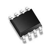
M95320-WMN6 STMicroelectronics, M95320-WMN6 Datasheet - Page 8

M95320-WMN6
Manufacturer Part Number
M95320-WMN6
Description
EEPROM 5.5V 32K (4Kx8)
Manufacturer
STMicroelectronics
Datasheet
1.M95320-RMB6TG.pdf
(44 pages)
Specifications of M95320-WMN6
Memory Size
32 Kbit
Organization
4 K x 8
Interface Type
SPI
Maximum Clock Frequency
5 MHz
Access Time
60 ns
Supply Voltage (max)
5.5 V
Supply Voltage (min)
2.5 V
Maximum Operating Current
4 mA
Maximum Operating Temperature
+ 85 C
Mounting Style
SMD/SMT
Package / Case
SO-8
Minimum Operating Temperature
- 40 C
Operating Supply Voltage
2.5 V, 5.5 V
Operating Temperature
- 40 C to + 85 C
Lead Free Status / Rohs Status
No
Available stocks
Company
Part Number
Manufacturer
Quantity
Price
Part Number:
M95320-WMN6
Manufacturer:
ST
Quantity:
20 000
Part Number:
M95320-WMN6P
Manufacturer:
ST
Quantity:
20 000
Company:
Part Number:
M95320-WMN6T
Manufacturer:
NIHON
Quantity:
990
Part Number:
M95320-WMN6T
Manufacturer:
ST
Quantity:
20 000
Company:
Part Number:
M95320-WMN6TP
Manufacturer:
ST
Quantity:
2 423
Company:
Part Number:
M95320-WMN6TP
Manufacturer:
STM
Quantity:
202
Part Number:
M95320-WMN6TP
Manufacturer:
ST
Quantity:
20 000
Signal description
2
2.1
2.2
2.3
2.4
2.5
8/44
Signal description
During all operations, V
V
All of the input and output signals must be held high or low (according to voltages of V
V
Serial Data output (Q)
This output signal is used to transfer data serially out of the device. Data is shifted out on the
falling edge of Serial Clock (C).
Serial Data input (D)
This input signal is used to transfer data serially into the device. It receives instructions,
addresses, and the data to be written. Values are latched on the rising edge of Serial Clock
(C).
Serial Clock (C)
This input signal provides the timing of the serial interface. Instructions, addresses, or data
present at Serial Data Input (D) are latched on the rising edge of Serial Clock (C). Data on
Serial Data Output (Q) changes after the falling edge of Serial Clock (C).
Chip Select (S)
When this input signal is high, the device is deselected and Serial Data output (Q) is at high
impedance. Unless an internal Write cycle is in progress, the device will be in the Standby
Power mode. Driving Chip Select (S) low selects the device, placing it in the Active Power
mode.
After Power-up, a falling edge on Chip Select (S) is required prior to the start of any
instruction.
Hold (HOLD)
The Hold (HOLD) signal is used to pause any serial communications with the device without
deselecting the device.
During the Hold condition, the Serial Data output (Q) is high impedance, and Serial Data
input (D) and Serial Clock (C) are Don’t Care.
To start the Hold condition, the device must be selected, with Chip Select (S) driven low.
OH
CC
(min) to V
, V
IL
or V
OL
CC
, as specified in
(max).
CC
must be held stable and within the specified valid range:
Doc ID 5711 Rev 12
Table 13
to
Table
16). These signals are described next.
M95320, M95320-W, M95320-R
IH
,


