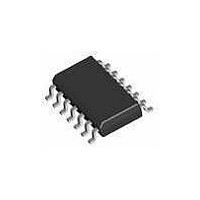
74LVC02AD NXP Semiconductors, 74LVC02AD Datasheet - Page 5

74LVC02AD
Manufacturer Part Number
74LVC02AD
Description
Gates (AND / NAND / OR / NOR) 3.3V QUAD 2-INPUT NOR GATE
Manufacturer
NXP Semiconductors
Datasheet
1.74LVC02ABQ115.pdf
(15 pages)
Specifications of 74LVC02AD
Product
NOR
Logic Family
LVC
Number Of Gates
Quad
Number Of Lines (input / Output)
2 / 1
High Level Output Current
- 24 mA
Low Level Output Current
24 mA
Propagation Delay Time
2.1 ns
Supply Voltage (max)
3.6 V
Supply Voltage (min)
1.2 V
Maximum Operating Temperature
+ 125 C
Mounting Style
SMD/SMT
Package / Case
SOT-108
Minimum Operating Temperature
- 40 C
Lead Free Status / Rohs Status
Details
Other names
74LVC02AD,112
Available stocks
Company
Part Number
Manufacturer
Quantity
Price
Company:
Part Number:
74LVC02AD
Manufacturer:
NXP40
Quantity:
5 000
Part Number:
74LVC02AD
Manufacturer:
NXP/恩智浦
Quantity:
20 000
Part Number:
74LVC02AD,118
Manufacturer:
NEXPERIA/安世
Quantity:
20 000
Company:
Part Number:
74LVC02ADB
Manufacturer:
PHI
Quantity:
2 500
Company:
Part Number:
74LVC02ADЈ¬118
Manufacturer:
NXP
Quantity:
57 500
Philips Semiconductors
RECOMMENDED OPERATING CONDITIONS
LIMITING VALUES
In accordance with the absolute maximum rating system (IEC 60134); voltages are referenced to GND (ground = 0 V).
Notes
1. The input and output voltage ratings may be exceeded if the input and output current ratings are observed.
2. For SO14 packages: above 70 C derate linearly with 8 mW/K.
2004 Mar 12
handbook, halfpage
V
V
V
T
t
V
I
V
I
V
I
I
T
P
SYMBOL
SYMBOL
r
IK
OK
O
CC
, t
amb
stg
CC
I
O
CC
I
O
tot
Quad 2-input NOR gate
f
, I
For SSOP and TSSOP14 packages: above 60 C derate linearly with 5.5 mW/K.
For DHVQFN14 packages: above 60 C derate linearly with 4.5 mW/K.
GND
Fig.5 Logic diagram (one gate).
A
B
supply voltage
input voltage
output voltage
operating ambient temperature
input rise and fall times
supply voltage
input diode current
input voltage
output diode current
output voltage
output source or sink current
V
storage temperature
power dissipation
CC
or GND current
PARAMETER
PARAMETER
MNA215
Y
for maximum speed performance
for low-voltage applications
V
V
V
note 1
V
note 1
V
T
amb
CC
CC
I
O
O
< 0 V
> V
= 0 V to V
= 1.2 V to 2.7 V
= 2.7 V to 3.6 V
= 40 C to +125 C; note 2
CC
CONDITIONS
CONDITIONS
or V
5
CC
O
< 0 V
2.7
1.2
0
0
0
0
40
0.5
0.5
0.5
65
MIN.
MIN.
3.6
3.6
5.5
V
+125
20
10
+6.5
+6.5
V
+150
500
50
50
50
100
CC
CC
Product specification
MAX.
MAX.
74LVC02A
+ 0.5 V
V
V
V
V
ns/V
ns/V
V
mA
V
mA
mA
mA
mW
C
C
UNIT
UNIT


