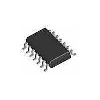
74LVC02AD NXP Semiconductors, 74LVC02AD Datasheet - Page 4

74LVC02AD
Manufacturer Part Number
74LVC02AD
Description
Gates (AND / NAND / OR / NOR) 3.3V QUAD 2-INPUT NOR GATE
Manufacturer
NXP Semiconductors
Datasheet
1.74LVC02ABQ115.pdf
(15 pages)
Specifications of 74LVC02AD
Product
NOR
Logic Family
LVC
Number Of Gates
Quad
Number Of Lines (input / Output)
2 / 1
High Level Output Current
- 24 mA
Low Level Output Current
24 mA
Propagation Delay Time
2.1 ns
Supply Voltage (max)
3.6 V
Supply Voltage (min)
1.2 V
Maximum Operating Temperature
+ 125 C
Mounting Style
SMD/SMT
Package / Case
SOT-108
Minimum Operating Temperature
- 40 C
Lead Free Status / Rohs Status
Details
Other names
74LVC02AD,112
Available stocks
Company
Part Number
Manufacturer
Quantity
Price
Company:
Part Number:
74LVC02AD
Manufacturer:
NXP40
Quantity:
5 000
Part Number:
74LVC02AD
Manufacturer:
NXP/恩智浦
Quantity:
20 000
Part Number:
74LVC02AD,118
Manufacturer:
NEXPERIA/安世
Quantity:
20 000
Company:
Part Number:
74LVC02ADB
Manufacturer:
PHI
Quantity:
2 500
Company:
Part Number:
74LVC02ADЈ¬118
Manufacturer:
NXP
Quantity:
57 500
Philips Semiconductors
2004 Mar 12
handbook, halfpage
handbook, halfpage
Quad 2-input NOR gate
Fig.1 Pin configuration SO14 and (T)SSOP14.
GND
1Y
1A
1B
2Y
2A
2B
11
12
Fig.3 Logic symbol.
2
3
5
6
8
9
1
2
3
4
5
6
7
1A
1B
2A
2B
3A
3B
4A
4B
02
MNA214
MNA216
1Y
2Y
3Y
4Y
14
13
12
11
10
9
8
13
10
4
1
V CC
4Y
4B
4A
3Y
3B
3A
4
handbook, halfpage
handbook, halfpage
(1) The die substrate is attached to this pad using conductive die
attach material. It can not be used as a supply pin or input.
Fig.2 Pin configuration DHVQFN14.
1A
1B
2Y
2A
2B
Fig.4 Logic symbol (IEEE/IEC).
Top view
2
3
4
5
6
11
12
2
3
5
6
8
9
GND
1Y
7
1
GND
MNA217
1
1
1
1
V CC
(1)
3A
14
8
10
13
Product specification
MNA951
1
4
74LVC02A
13
12
11
10
9
4Y
4B
4A
3Y
3B


