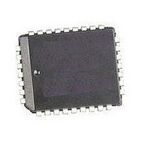
M50FW040K1 STMicroelectronics, M50FW040K1 Datasheet - Page 30

M50FW040K1
Manufacturer Part Number
M50FW040K1
Description
Flash 3.6V 4M (512Kx8)
Manufacturer
STMicroelectronics
Datasheet
1.M50FW040K1.pdf
(41 pages)
Specifications of M50FW040K1
Data Bus Width
8 bit
Memory Type
NOR
Memory Size
4 Mbit
Architecture
Sectored
Interface Type
Firmware Hub
Access Time
11 ns, 50 ns
Supply Voltage (max)
3.6 V
Supply Voltage (min)
3 V
Maximum Operating Current
20 mA
Operating Temperature
+ 70 C
Mounting Style
SMD/SMT
Package / Case
PLCC-32
Organization
512 KB x 8
Lead Free Status / Rohs Status
No
Available stocks
Company
Part Number
Manufacturer
Quantity
Price
Company:
Part Number:
M50FW040K1
Manufacturer:
ST
Quantity:
3 112
Company:
Part Number:
M50FW040K1
Manufacturer:
STM
Quantity:
245
Company:
Part Number:
M50FW040K1
Manufacturer:
QP-SEMI
Quantity:
13
Part Number:
M50FW040K1
Manufacturer:
ST
Quantity:
20 000
Company:
Part Number:
M50FW040K1T
Manufacturer:
TI
Quantity:
125
Part Number:
M50FW040K1T
Manufacturer:
ST
Quantity:
20 000
M50FW040
Figure 15. A/A Mux Interface Write AC Waveforms
Table 23. A/A Mux Interface Write AC Characteristics
Note: 1. Sampled only, not 100% tested.
30/41
t
t
QVVPL
VPHWH
Symbol
t
t
t
t
t
t
t
t
t
t
t
WLWH
WHWL
CHWH
DVWH
WHDX
WHGL
CHAX
WHRL
AVCH
AVCL
CLAX
A0-A10
RC
W
G
RB
V PP
DQ0-DQ7
2. Applicable if V
(1,2)
(1)
Write Enable Low to Write Enable High
Data Valid to Write Enable High
Write Enable High to Data Transition
Row Address Valid to RC Low
RC Low to Row Address Transition
Column Address Valid to RC High
RC High to Column Address Transition
Write Enable High to Write Enable Low
RC High to Write Enable High
V
Write Enable High to Output Enable Low
Write Enable High to RB Low
Output Valid, RB High to V
PP
High to Write Enable High
PP
tWLWH
is seen as a logic input (V
Write erase or
program setup
R1
tAVCL
Parameter
tWHWL
tCLAX
C1
D IN1
PP
valid address and data
Write erase confirm or
tAVCH
Low
R2
PP
tVPHWH
tDVWH
< 3.6V).
tCHAX
tWHRL
C2
D IN2
tCHWH
Automated erase
or program delay
Test Condition
tWHDX
tWHGL
Register Data
Read Status
Min
Min
Min
Min
Min
Min
Min
Min
Min
Min
Min
Min
Min
VALID SRD
tQVVPL
Value
another command
100
100
100
50
50
50
50
50
50
30
0
Ready to write
5
0
AI04185
Unit
ns
ns
ns
ns
ns
ns
ns
ns
ns
ns
ns
ns
ns


