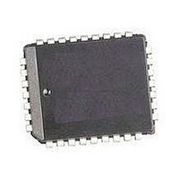
M50FW040K1 STMicroelectronics, M50FW040K1 Datasheet - Page 11

M50FW040K1
Manufacturer Part Number
M50FW040K1
Description
Flash 3.6V 4M (512Kx8)
Manufacturer
STMicroelectronics
Datasheet
1.M50FW040K1.pdf
(41 pages)
Specifications of M50FW040K1
Data Bus Width
8 bit
Memory Type
NOR
Memory Size
4 Mbit
Architecture
Sectored
Interface Type
Firmware Hub
Access Time
11 ns, 50 ns
Supply Voltage (max)
3.6 V
Supply Voltage (min)
3 V
Maximum Operating Current
20 mA
Operating Temperature
+ 70 C
Mounting Style
SMD/SMT
Package / Case
PLCC-32
Organization
512 KB x 8
Lead Free Status / Rohs Status
No
Available stocks
Company
Part Number
Manufacturer
Quantity
Price
Company:
Part Number:
M50FW040K1
Manufacturer:
ST
Quantity:
3 112
Company:
Part Number:
M50FW040K1
Manufacturer:
STM
Quantity:
245
Company:
Part Number:
M50FW040K1
Manufacturer:
QP-SEMI
Quantity:
13
Part Number:
M50FW040K1
Manufacturer:
ST
Quantity:
20 000
Company:
Part Number:
M50FW040K1T
Manufacturer:
TI
Quantity:
125
Part Number:
M50FW040K1T
Manufacturer:
ST
Quantity:
20 000
BUS OPERATIONS
The two interfaces have similar bus operations but
the signals and timings are completely different.
The Firmware Hub (FWH) Interface is the usual in-
terface and all of the functionality of the part is
available through this interface. Only a subset of
functions are available through the Address/Ad-
dress Multiplexed (A/A Mux) Interface.
Follow the section
erations
Multiplexed (A/A Mux) Bus Operations
description of the bus operations on each inter-
face.
Firmware Hub (FWH) Bus Operations
The Firmware Hub (FWH) Interface consists of
four data signals (FWH0-FWH3), one control line
(FWH4) and a clock (CLK). In addition protection
against accidental or malicious data corruption
can be achieved using two further signals (TBL
and WP). Finally two reset signals (RP and INIT)
are available to put the memory into a known
state.
The data signals, control signal and clock are de-
signed to be compatible with PCI electrical specifi-
cations. The interface operates with clock speeds
up to 33MHz.
The following operations can be performed using
the appropriate bus cycles: Bus Read, Bus Write,
Standby, Reset and Block Protection.
Bus Read. Bus Read operations read from the
memory cells, specific registers in the Command
Interface or Firmware Hub Registers. A valid Bus
Read operation starts when Input Communication
Frame, FWH4, is Low, V
correct Start cycle is on FWH0-FWH3. On the fol-
lowing clock cycles the Host will send the Memory
ID Select, Address and other control bits on
FWH0-FWH3. The memory responds by output-
ting Sync data until the wait-states have elapsed
followed by Data0-Data3 and Data4-Data7.
Refer to
tions, and
for a description of the Field definitions for each
clock cycle of the transfer. See
terface AC Signal Timing
ure 12., FWH
Waveforms, for details on the timings of the sig-
nals.
Bus Write. Bus Write operations write to the
Command Interface or Firmware Hub Registers. A
valid Bus Write operation starts when Input Com-
munication Frame, FWH4, is Low, V
rises and the correct Start cycle is on FWH0-
FWH3. On the following Clock cycles the Host will
send the Memory ID Select, Address, other control
bits, Data0-Data3 and Data4-Data7 on FWH0-
below and the section
Table 4., FWH Bus Read Field Defini-
Figure 7., FWH Bus Read
Interface
Firmware Hub (FWH) Bus Op-
IL
Characteristics, and
, as Clock rises and the
AC Signal
Table 20., FWH In-
Address/Address
Waveforms,
IL
below for a
, as Clock
Timing
Fig-
FWH3. The memory outputs Sync data until the
wait-states have elapsed.
Refer to
tions, and
for a description of the Field definitions for each
clock cycle of the transfer. See
terface AC Signal Timing
ure 12., FWH
Waveforms, for details on the timings of the sig-
nals.
Bus Abort. The Bus Abort operation can be used
to immediately abort the current bus operation. A
Bus Abort occurs when FWH4 is driven Low, V
during the bus operation; the memory will tri-state
the Input/Output Communication pins, FWH0-
FWH3.
Note that, during a Bus Write operation, the Com-
mand Interface starts executing the command as
soon as the data is fully received; a Bus Abort dur-
ing the final TAR cycles is not guaranteed to abort
the command; the bus, however, will be released
immediately.
Standby. When FWH4 is High, V
is put into Standby mode where FWH0-FWH3 are
put into a high-impedance state and the Supply
Current is reduced to the Standby level, I
Reset. During Reset mode all internal circuits are
switched off, the memory is deselected and the
outputs are put in high-impedance. The memory is
in Reset mode when Interface Reset, RP, or CPU
Reset, INIT, is Low, V
Low, V
mode upon return from Reset mode and the Lock
Registers return to their default states regardless
of their state before Reset, see
INIT goes Low, V
eration, the operation is aborted and the memory
cells affected no longer contain valid data; the
memory can take up to t
or Erase operation.
Block Protection. Block
forced using the signals Top Block Lock, TBL, and
Write Protect, WP, regardless of the state of the
Lock Registers.
Address/Address Multiplexed (A/A Mux) Bus
Operations
The Address/Address Multiplexed (A/A Mux) Inter-
face has a more traditional style interface. The sig-
nals consist of a multiplexed address signals (A0-
A10), data signals, (DQ0-DQ7) and three control
signals (RC, G, W). An additional signal, RP, can
be used to reset the memory.
The Address/Address Multiplexed (A/A Mux) Inter-
face is included for use by Flash Programming
equipment for faster factory programming. Only a
IL
, for t
Table 5., FWH Bus Write Field Defini-
Figure 8., FWH Bus Write
PLPH
IL
Interface
, during a Program or Erase op-
. The memory resets to Read
IL
. RP or INIT must be held
PLRH
Characteristics, and
Protection
AC Signal
to abort a Program
Table 20., FWH In-
Table 10.
IH
, the memory
M50FW040
Waveforms,
can
CC1
If RP or
Timing
.
11/41
Fig-
be
IL
,


