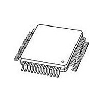
"CX24109-11Z,518" NXP Semiconductors, "CX24109-11Z,518" Datasheet - Page 35

"CX24109-11Z,518"
Manufacturer Part Number
"CX24109-11Z,518"
Description
Manufacturer
NXP Semiconductors
Datasheet
1.CX24109-11Z518.pdf
(40 pages)
Specifications of "CX24109-11Z,518"
Lead Free Status / Rohs Status
Compliant
NXP Semiconductors
Table 15.
CX24109_N_1
Product data sheet
Reference Oscillator Phase Noise
Spurious
VCO Tuning Sensitivity
LO Phase Noise at 950 MHz–1450 MHz
LO Phase Noise at 1450 MHz–2150 MHz
LO Phase Noise at 950 MHz–2150 MHz
Local Oscillator Settling Time
GENERAL NOTES:
1. Values in this table are valid under the operating conditions listed in
FOOTNOTES:
(1)
(2)
(3)
(4)
(5)
(6)
(7)
(8)
(9)
stated.
This measurement is made at RFIN of CX24109.
Aggregate average power of 40 QPSK modulated carriers.
All NF and IIP3 measurements/specifications are made by setting a specific input level for the desired symbol rate and adjusting the AGC
level to obtain the desired output level of 0.5 Vpp.
This level is derived assuming –23 dBm is the maximum level of all other transponders and that the operating symbol rate is 1 MSps.
Assume C/I of 7 dB and a bandwidth scaling of 10 log (20 MHz / 1 MHz), thus, Pin = –23 dBm – 7 dB – 10 log (20 / 1) = –43 dBm.
This level is derived from Pin = P
P
45 dB – 20 dB = –81 dBm.
This level is derived assuming –23 dBm is the maximum level of all other transponders and that the operating symbol rate is 7 MSps.
Assume C/I of 7 dB and a bandwidth scaling of 10 log (20 MHz / 7 MHz), thus, Pin = –23 dBm – 7 dB – 10 log 20 / 7 = –34.5 dBm.
This level is derived from Pin = P
P
This level is derived assuming –23 dBm is the maximum level of all other transponders, an operating symbol rate of 20 MSps and a C/I of
7 dB.
Assume a symbol rate of 20 MSps.
Transponder
Transponder
RF Electrical Characteristics (Sheet 3 of 3)
is at a minimum. P
= 10 log ((7E6 / 45E6) 10
Parameter
Transponder
Transponder
Transponder
(82–4)/10
= 10 log ((1E6 / 45E6) 10
– L
– L
) = +70 dBm. Therefore, Pin = +70 dB – 205 dB + 38 dB + 45 dB – 20 dB = –72 dBm
Path
Path
+ G
+ G
Rev. 01 — 13 November 2008
Measured at 400 Hz
At 1, 10.111, and 30 MHz offsets
with 2 mA charge pump and
10 kHz loop BW
10 kHz offset
100 kHz offset
10 kHz offset
100 kHz offset
10 kHz offset +100 kHz offset
All frequencies, VCOs and modes
VCO and Synthesizer
Antenna
Antenna
+ G
+ G
LNBmin
LNBmin
(82 – 4) /10
Tables 8, 9,
Conditions
– L
– L
—
Cable
Cable
) = +61 dBm. Therefore, Pin = + 61 dBm – 205 dB + 38 dB +
Chapter 3: Parametric Data and Specifications
and
. Where the operating symbol rate is 1 MSps and
. Where the operating symbol rate is 7 MSps and
10
,
using a reference divider of 10, unless otherwise
Min
–30
100
—
—
—
—
—
—
—
–130
Typ
–45
–75
–97
–69
–94
—
—
1
CX24109
–158
Max
© NXP B.V. 2008. All rights reserved.
330
—
—
—
—
—
—
—
dBc/Hz
dBc/Hz
dBc/Hz
dBc/Hz
dBc/Hz
dBc/Hz
MHz/V
Units
dBc
ms
35


