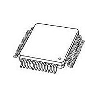
"CX24109-11Z,518" NXP Semiconductors, "CX24109-11Z,518" Datasheet - Page 32

"CX24109-11Z,518"
Manufacturer Part Number
"CX24109-11Z,518"
Description
Manufacturer
NXP Semiconductors
Datasheet
1.CX24109-11Z518.pdf
(40 pages)
Specifications of "CX24109-11Z,518"
Lead Free Status / Rohs Status
Compliant
NXP Semiconductors
Table 13.
Table 14.
CX24109_N_1
Product data sheet
Supply Current
Usable AGC Voltage Range, V
Impedance of AGC Input
AGC Current, I
Usable Filtune Voltage Range, V
Impedance of Filtune Input
Thermal Resistance of Package
FOOTNOTES:
(1)
(2)
Bus Timing
Programming Lines:
Clock, Data, Enable
LD and CLKREFOUT
Using 15–45 MSps programming values (see
Using a 2-layer CX24109/CX24121 reference design, where the package’s exposed paddle is connected to the printed circuit board ground plane
using thermal vias. The ground plane on the reference design is approximately 2-7/8 inches x 1-1/4 inches. Better thermal performance can be
obtained by increasing ground plane coverage or increasing the number of attached printed circuit board layers.
Programming Clock Frequency
DC Electrical Characteristics
AC Electrical Characteristics
AGC
(1)
Parameter
Parameter
AGC
Filtune
Clock to Enable,
Data Setup, t
Data Hold, t
Enable Pulse
Width, t
V
V
t
V
V
I
I
CE
IH
OH
IL
OL
IH
IL
Table
EW
HD
SU
8), V
Rev. 01 — 13 November 2008
cc
= 5.0 V, V
Conditions
AGC
at DC
at DC
θja
θjc
—
—
—
—
(2)
= 1.45 V, V
See
Conditions
Figure
Chapter 3: Parametric Data and Specifications
—
—
—
—
—
—
—
Filtune
15.
= 2.7 V.
Min
1.3
—
—
—
—
—
—
0
Min
2.1
2.3
—
—
—
—
—
—
—
—
1
Typ
244
8.7
17
42
—
—
—
1
Typ
2.65
0.9
10
10
—
—
—
—
—
—
CX24109
1
© NXP B.V. 2008. All rights reserved.
Max
2.80
262
0.4
3.0
—
—
—
—
1.125
Max
–0.5
0.8
0.5
—
—
—
—
—
—
1
Units
°C/W
°C/W
MΩ
mA
mA
kΩ
Units
MHz
V
V
mA
mA
μs
μs
ns
ns
V
V
V
V
32


