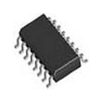
LTC1235CS Linear Technology, LTC1235CS Datasheet - Page 9

LTC1235CS
Manufacturer Part Number
LTC1235CS
Description
Manufacturer
Linear Technology
Datasheet
1.LTC1235CS.pdf
(16 pages)
Specifications of LTC1235CS
Number Of Elements
1
Monitored Voltage 1 (typ)
4.65V
Battery Backup Switching
Yes
Watchdog Timer
Yes
Chip Enable Signals
Yes
Reset Active Time
280ms
Manual Reset
Yes
Package Type
SOL
Operating Supply Voltage (min)
4.75V
Operating Supply Voltage (max)
5.5V
Reset Threshold Voltage (max)
4.75V
Reset Threshold Voltage (min)
4.5V
Power Dissipation
500mW
Operating Temp Range
0C to 70C
Operating Temperature Classification
Commercial
Power Fail Detection
Yes
Mounting
Surface Mount
Pin Count
16
Supply Current
1.5mA
Lead Free Status / Rohs Status
Not Compliant
Available stocks
Company
Part Number
Manufacturer
Quantity
Price
Part Number:
LTC1235CS
Manufacturer:
LINEAR/凌特
Quantity:
20 000
Part Number:
LTC1235CS#TRPBF
Manufacturer:
LTNEAR
Quantity:
20 000
Part Number:
LTC1235CSW
Manufacturer:
LINEAR/凌特
Quantity:
20 000
Part Number:
LTC1235CSW#PBF
Manufacturer:
LINEAR/凌特
Quantity:
20 000
Part Number:
LTC1235CSW#TR
Manufacturer:
LT/凌特
Quantity:
20 000
APPLICATIONS INFORMATION
Voltage Output
During normal operation, the LTC1235 uses a charge
pumped NMOS power switch to achieve low dropout and
low supply current. This power switch can deliver up to
50mA to V
of 5. The V
0.1μF or greater to ensure stability. Use of a larger bypass
capacitor is advantageous for supplying current to heavy
transient loads.
When operating currents larger than 50mA are required
from V
ential) is desired, the LTC1235 provides BATT ON output
to drive the base of external PNP transistor (Figure 3).
Another alternative to provide higher current is to connect
a high current Schottky diode from the V
pin to supply the extra current.
The LTC1235 is protected for safe area operation with short
circuit limit. Output current is limited to approximately
200mA. If the device is overloaded for a long period of
time, thermal shutdown turns the power switch off until
the device cools down. The threshold temperature for
thermal shutdown is approximately 155°C with about 10°C
of hysteresis which prevents the device from oscillating
in and out of shutdown.
The PNP switch was not chosen for the internal power
switch because it injects unwanted current into the
substrate. This current is collected by the V
competitive devices and adds to the charging current of
Figure 3. Using BATT ON to Drive External PNP Transistor
OUT
+5V
, or a lower dropout (V
OUT
OUT
0.1μF
pin should be bypassed with a capacitor of
from V
+3V
CC
V
V
and has a typical on resistance
BATT
CC
LTC1235
BATT ON
ANY PNP POWER TRANSISTOR
GND
R1
V
OUT
CC
- V
OUT
CC
0.1μF
pin to the V
voltage differ-
1235 F03
BATT
pin in
OUT
the battery which can damage lithium batteries. LTC1235
uses a charge pumped NMOS power switch to eliminate
unwanted charging current while achieving low dropout
and low supply current. Since no current goes to the
substrate, the current collected by V
junction leakage.
Conditional Battery Backup
LTC1235 provides an unique feature to either allow V
be switched to V
backup function when primary power is lost. Disabling
the battery backup function is useful in conserving the
backup battery’s life when the SRAM doesn’t need battery
backup during long term storage of a computer system,
or delivery of the computer system to the end user.
The BACKUP pin (Pin 8) is used to serve this feature on
power-down. When V
age threshold, the status of the BACKUP pin (logic low
or logic high) is stored in the Memory Logic (see Block
Diagram). If the stored status is logic high and V
50mV greater than V
nects the V
comparator, C2, shuts off the NMOS power switch, M1. M2
is designed for very low dropout voltage (input-to-output
differential). This feature is advantageous for low current
applications such as battery backup in CMOS RAM and
other low power CMOS circuitry. If the stored status is
logic low and V
Memory Logic keeps M2 off and C2 shuts off M1. V
in Battery Saving Mode (see Figure 4). The supply current
in both mode is 1μA maximum.
On power-ups, C2 keeps M1 off before V
higher than V
tery is replaced (with power off), the status stored in the
Memory Logic is undetermined. V
Battery Backup Mode or in Battery Saving Mode. When
V
C2 has typically 20mV of hysteresis to prevent spurious
switching when V
status stored in the Memory Logic is high. The response
time of C2 is approximately 20μs.
CC
is 70mV greater than V
BATT
BATT
CC
BATT
input to V
CC
. On the fi rst power-up after the bat-
falls to 50mV greater than V
remains nearly equal to V
BATT
or to disable the CMOS RAM battery
CC
, a 125Ω PMOS switch, M2, con-
is falling through the reset volt-
OUT
BATT
and the battery switchover
, M1 connects V
OUT
BATT
could be either in
LTC1235
CC
reaches 70mV
pin is strictly
BATT
OUT
BATT
CC
and the
to V
OUT
OUT
fall to
, the
1235fa
9
CC
to
is
.


