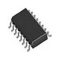
LTC1235CS Linear Technology, LTC1235CS Datasheet - Page 11

LTC1235CS
Manufacturer Part Number
LTC1235CS
Description
Manufacturer
Linear Technology
Datasheet
1.LTC1235CS.pdf
(16 pages)
Specifications of LTC1235CS
Number Of Elements
1
Monitored Voltage 1 (typ)
4.65V
Battery Backup Switching
Yes
Watchdog Timer
Yes
Chip Enable Signals
Yes
Reset Active Time
280ms
Manual Reset
Yes
Package Type
SOL
Operating Supply Voltage (min)
4.75V
Operating Supply Voltage (max)
5.5V
Reset Threshold Voltage (max)
4.75V
Reset Threshold Voltage (min)
4.5V
Power Dissipation
500mW
Operating Temp Range
0C to 70C
Operating Temperature Classification
Commercial
Power Fail Detection
Yes
Mounting
Surface Mount
Pin Count
16
Supply Current
1.5mA
Lead Free Status / Rohs Status
Not Compliant
Available stocks
Company
Part Number
Manufacturer
Quantity
Price
Part Number:
LTC1235CS
Manufacturer:
LINEAR/凌特
Quantity:
20 000
Part Number:
LTC1235CS#TRPBF
Manufacturer:
LTNEAR
Quantity:
20 000
Part Number:
LTC1235CSW
Manufacturer:
LINEAR/凌特
Quantity:
20 000
Part Number:
LTC1235CSW#PBF
Manufacturer:
LINEAR/凌特
Quantity:
20 000
Part Number:
LTC1235CSW#TR
Manufacturer:
LT/凌特
Quantity:
20 000
Table 1 shows the state of each pin during battery backup.
If the backup battery is not used, connect V
and V
Table 1. Input and Output Status in Battery Backup Mode
SIGNAL
V
BACKUP
V
V
BATT ON
PFI
PFO
PB RST
RESET
RESET
LOW LINE Logic low
WDI
WDO
CE IN
CE OUT
Memory Protection
The LTC1235 includes memory protection circuitry which
ensures the integrity of the data in memory by preventing
write operations when V
CC
OUT
BATT
OUT
STATUS
C2 monitors V
BACKUP is ignored.
V
The supply current is 1μA maximum.
Logic high. The open circuit output voltage is equal to V
Power Failure Input is ignored.
Logic low
PB RST is ignored.
Logic low
Logic high. The open circuit output voltage is equal to V
Watchdog Input is ignored.
Logic high. The open circuit output voltage is equal to V
Chip Enable Input is ignored.
Logic high. The open circuit output voltage is equal to V
to V
OUT
CC
is connected to V
BACKUP = V
CE OUT
.
CE IN
V
CC
CC
V
OUT
for active switchover.
CC
CC
= V
BATT
is at invalid level. Two pins, CE
BATT
through an internal PMOS switch.
Figure 6. Timing Diagram for CE IN and CE OUT
BATT
to GND
V1
OUT
OUT
OUT
OUT
.
.
.
.
V2
IN and CE OUT, control the Chip Enable or Write inputs of
CMOS RAM. When V
a typical propagation delay of 20ns. When V
the reset voltage threshold or V
high, independent of CE IN. CE OUT is an alternative signal
to drive the CE, CS, or Write input of battery-backed up
CMOS RAM. CE OUT can also be used to drive the Store
or Write input of an EEPROM, EAROM or NOVRAM to
achieve similar protection. Figure 6 shows the timing
diagram of CE IN and CE OUT.
CE IN can be derived from the microprocessor’s address
decoder output. Figure 7 shows a typical nonvolatile CMOS
RAM application.
+5V
0.1μF
+3V
V1 = RESET VOLTAGE THRESHOLD
V2 = RESET VOLTAGE THRESHOLD +
Figure 7. A Typical Nonvolatile CMOS RAM Application
RESET THRESHOLD HYSTERESIS
V
V
BATT
CC
GND
LTC1235
BACKUP
CE OUT
RESET
CE IN
V
OUT
CC
is +5V, CE OUT follows CE IN with
+
20ns PROPAGATION DELAY
FROM DECODER
TO μP
10μF
V
BATT
OUT
= V
1235 F06
, CE OUT is forced
BATT
LTC1235
0.1μF
CC
falls below
CS
V
CC
62512
GND
RAM
11
1235 F07
1235fa


