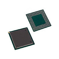
XPC850ZT50B Freescale Semiconductor, XPC850ZT50B Datasheet - Page 11

XPC850ZT50B
Manufacturer Part Number
XPC850ZT50B
Description
Manufacturer
Freescale Semiconductor
Datasheet
1.XPC850ZT50B.pdf
(76 pages)
Specifications of XPC850ZT50B
Family Name
MPC8xx
Device Core
PowerQUICC
Device Core Size
32b
Frequency (max)
50MHz
Instruction Set Architecture
RISC
Supply Voltage 1 (typ)
3.3V
Operating Supply Voltage (max)
3.465V
Operating Supply Voltage (min)
3.135V
Operating Temp Range
0C to 95C
Operating Temperature Classification
Commercial
Mounting
Surface Mount
Pin Count
256
Package Type
BGA
Lead Free Status / Rohs Status
Not Compliant
Available stocks
Company
Part Number
Manufacturer
Quantity
Price
Company:
Part Number:
XPC850ZT50B
Manufacturer:
SHARP
Quantity:
686
Part Number:
XPC850ZT50B
Manufacturer:
MOTOROLA/摩托罗拉
Quantity:
20 000
Part Number:
XPC850ZT50B-0K24A
Manufacturer:
MOTOROLA/摩托罗拉
Quantity:
20 000
Part Number:
XPC850ZT50BU
Manufacturer:
MOTOROLA/摩托罗拉
Quantity:
20 000
P
For most applications P
approximate relationship between P
Solving equations (1) and (2) for K gives:
where K is a constant pertaining to the particular part. K can be determined from equation
(3) by measuring P
P
5.1
Each V
supply. Each GND pin should likewise be provided with a low-impedance path to ground.
The power supply pins drive distinct groups of logic on chip. The V
be bypassed to ground using at least four 0.1 µF by-pass capacitors located as close as
possible to the four sides of the package. The capacitor leads and associated printed circuit
traces connecting to chip V
lead. A four-layer board is recommended, employing two inner layers as V
planes.
All output pins on the MPC850 have fast rise and fall times. Printed circuit (PC) trace
interconnection length should be minimized in order to minimize undershoot and
reflections caused by these fast output switching times. This recommendation particularly
applies to the address and data busses. Maximum PC trace lengths of six inches are
recommended. Capacitance calculations should consider all device loads as well as
parasitic capacitances due to the PC traces. Attention to proper PCB layout and bypassing
becomes especially critical in systems with higher capacitive loads because these loads
create higher transient currents in the V
signals that will be inputs during reset. Special care should be taken to minimize the noise
levels on the PLL supply pins.
MOTOROLA
D
D
= P
and T
P
P
P
K = P
INT
I/O
D
INT
CC
= K ÷ (T
J
= Power dissipation on input and output pins—user determined
Layout Practices
+ P
= I
pin on the MPC850 should be provided with a low-impedance path to the board’s
can be obtained by solving equations (1) and (2) iteratively for any value of T
D
•
DD
I/O
(T
x V
A
J
+ 273°C)
+ 273°C) + θ
DD
D
,
(at equilibrium) for a known T
watts—chip internal power
Freescale Semiconductor, Inc.
MPC850 (Rev. A/B/C) Hardware Specifications
I/O
For More Information On This Product,
CC
< 0.3
and GND should be kept to less than half an inch per capacitor
JA
• P
Go to: www.freescale.com
•
D
D
P
and T
(2)
(3)
INT
CC
and can be neglected. If P
and GND circuits. Pull up all unused inputs or
J
is:
A
. Using this value of K
CC
power supply should
I/O
is neglected
Layout Practices
,
the values of
CC
and GND
,
A
an
11
.


