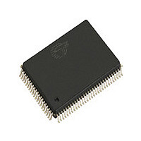
CY7C1363A-117AJC Cypress Semiconductor Corp, CY7C1363A-117AJC Datasheet - Page 28

CY7C1363A-117AJC
Manufacturer Part Number
CY7C1363A-117AJC
Description
Manufacturer
Cypress Semiconductor Corp
Datasheet
1.CY7C1363A-117AJC.pdf
(34 pages)
Specifications of CY7C1363A-117AJC
Density
9Mb
Access Time (max)
7ns
Sync/async
Synchronous
Architecture
SDR
Clock Freq (max)
117MHz
Operating Supply Voltage (typ)
3.3V
Address Bus
19b
Package Type
TQFP
Operating Temp Range
0C to 70C
Number Of Ports
1
Supply Current
320mA
Operating Supply Voltage (min)
3.135V
Operating Supply Voltage (max)
3.6V
Operating Temperature Classification
Commercial
Mounting
Surface Mount
Pin Count
100
Word Size
18b
Number Of Words
512K
Lead Free Status / Rohs Status
Not Compliant
Document #: 38-05302 Rev. *B
Timing Diagrams
Read/Write Cycle Timing
Notes:
23. The data bus (Q) remains in high-Z following a WRITE cycle, unless a new read access is initiated by ADSP or ADSC .
24. GW is HIGH.
25. Device must be deselected when entering ZZ mode. See Cycle Descriptions table for all possible signal conditions to deselect the device.
26. DQs are in high-Z when exiting ZZ sleep mode.
Data Out (Q)
Data In (D)
BWE, BW
ADDRESS
ADSP
ADSC
ADV
CLK
OE
CE
X
A1
High-Z
t ADS
Back-to-Back READs
t CES
t AS
(continued)
Q(A1)
A2
t ADH
[21, 23, 24]
t CEH
t
t AH
CH
t CYC
t
CL
Q(A2)
t
OEHZ
A3
Single WRITE
t
t DS
WES
D(A3)
t DH
t
WEH
DON’T CARE
A4
t OELZ
t CDV
Q(A4)
UNDEFINED
Q(A4+1)
BURST READ
Q(A4+2)
Q(A4+3)
CY7C1361B
CY7C1363B
D(A5)
Back-to-Back
A5
Page 28 of 34
WRITEs
D(A6)
A6
[+] Feedback


