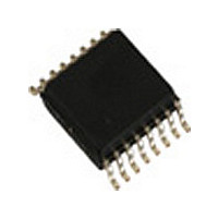
CY2DP814ZC Cypress Semiconductor Corp, CY2DP814ZC Datasheet - Page 5

CY2DP814ZC
Manufacturer Part Number
CY2DP814ZC
Description
Manufacturer
Cypress Semiconductor Corp
Datasheet
1.CY2DP814ZC.pdf
(9 pages)
Specifications of CY2DP814ZC
Number Of Outputs
8
Operating Supply Voltage (max)
3.465V
Operating Temp Range
0C to 70C
Propagation Delay Time
<4ns
Operating Supply Voltage (min)
3.135V
Mounting
Surface Mount
Pin Count
16
Operating Supply Voltage (typ)
3.3V
Package Type
TSSOP
Power Dissipation
750W
Input Frequency
450MHz
Operating Temperature Classification
Commercial
Lead Free Status / Rohs Status
Not Compliant
Available stocks
Company
Part Number
Manufacturer
Quantity
Price
Company:
Part Number:
CY2DP814ZC
Manufacturer:
SUN
Quantity:
103
Part Number:
CY2DP814ZC
Manufacturer:
CYPRESS/赛普拉斯
Quantity:
20 000
Table 10. High-frequency Parametrics
Notes
Document Number: 38-07060 Rev. *F
Fmax
Fmax(20)
TW
3. RL = 50 ohm1%; Zline = 50 ohm 6Ó.
4. CL includes instrumentation and fixture capacitance within 6 mm of the UT.
5. TPA and B are used for prop delay and rise/fall measurements. T
6. When measuring Tr/Tf, tpd, V
7. LVCMOS/LVTTL single-ended input value. Ground either input: when on the B side, non-inversion takes place. If A side is grounded, the signal becomes the complement
Parameter
of the input on B side. See
Figure 3. Differential Receiver to Driver Propagation Delay and Driver Transition Time
Maximum Frequency
V
Maximum Frequency
V
Minimum Pulse
V
DD
DD
DD
= 3.3V
= 3.3V
= 3.3V
Description
Table
OD
G enera tor
point T
3.
P ulse
E n2
E n1
PC
V 1A
V 1B
V 0Y
V 0Z
is held at V
Device concept
B
A
1 . 2 V C M
1 . 2 V C M
50% Duty Cycle tW(50–50)
Standard Load Circuit
20% Duty Cycle tW(20–80)
LVPECL Input
Vin = V
Vout = V
Vin = V
Vout = V
LVPECL Input
VDD
DD
Figure 2. Differential PECL Output
– 2.0V.
T
IH
IH
P L H
OH
OH
V 0 Y -
(Max.)/V
(Max.)/V
V 0 Z
(Min.)/V
(Min.)/V
PC
150
150
S tan dard T erm in ation
T
is used for V
P H L
IL
IL
Conditions
(Min.)
OL
(Min.) F = 100 MHz
OL
G N D
Q
Q
(Max.).(Limit)
(Max.) (Limit)
R
t
OC
measurements only and otherwise connected to V
User Defined
F
VTT & RTT
t
0 V D if f e r e n t ia l
0 V D if f e r e n t ia l
10pF
0 V D if f e r e n t ia l
1.4 V
1.0 V
1.4 V
1.0 V
8 0 %
2 0 %
VDD - 2V
T PA
T P C
T PB
50
50
Min
900
V D D -2V
Typ
[3, 4, 5, 6, 7]
DD
– 2.
Max
450
175
CY2DP814
Page 5 of 9
MHz
MHz
Unit
ps
[+] Feedback
[+] Feedback


