CY2DP814ZC Cypress Semiconductor Corp, CY2DP814ZC Datasheet
CY2DP814ZC
Specifications of CY2DP814ZC
Available stocks


Related parts for CY2DP814ZC

CY2DP814ZC Summary of contents
Page 1
... Industrial versions available ■ Available in TSSOP package ■ Logic Block Diagram Cypress Semiconductor Corporation Document Number: 38-07060 Rev. *F 1:4 Clock Fanout Buffer Description The Cypress CY2 series of network circuits are produced using advanced 0.35-micron CMOS technology, achieving the industry’s fastest logic. ...
Page 2
Pin Configuration Pin Description Pin Number Pin Name 6, 7 IN+, IN– 2 CONFIG 1, 8 EN1, EN2 16, 15, 14, 13, 12, 11, 10, 9 Q1A, Q1B, Q2A, Q2B, Q3A, Q3B, Q4A, Q4B GND ...
Page 3
Maximum Ratings [1, 2] Storage Temperature: ................................. –65C to +150C Ambient Temperature: .................................. –40C to +85C Supply Voltage to Ground Potential (Inputs and V only) .......................................–0.3V to 4.6V CC Table 1. EN1 EN2 Function Table Enable Logic EN1 EN2 H ...
Page 4
Table 6. DC Electrical Characteristics: 3.3V–LVPECL Input Parameter Description V Differential Input Voltage p VCM Common-mode Voltage I Input High Current IH I Input Low Current IL I Input High Current I Table 7. DC Electrical Characteristics: ...
Page 5
Device concept Table 10. High-frequency Parametrics Parameter Description Fmax Maximum Frequency V = 3.3V DD Fmax(20) Maximum Frequency Minimum Pulse V = 3.3V DD Figure 3. Differential Receiver to Driver Propagation Delay and Driver Transition ...
Page 6
Figure 4. Test Circuit and Voltage Definitions for the Driver Common-mode Output Voltage Figure 5. Test Circuit and Voltage Definitions ...
Page 7
Figure 6. Test Circuit and Voltage Definitions for the Driver Common-Mode Output Voltage P uls era uls nerator En1 En2 DE Q Figure 7. LVTTL/LVCMOS INPUT A LVCM OS / LVTTL ...
Page 8
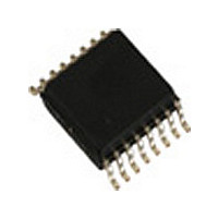
Package Drawing and Dimensions Figure 9. 16-Pin TSSOP 4.40 mm Body Z16.173 Note 10. LVPECL or LVDS differential input value. Document Number: 38-07060 Rev. *F CY2DP814 51-85091 *B Page [+] Feedback [+] Feedback ...
Page 9
... Removed pruned parts Added typical values RGL Added Lead-free for TSSOP Industrial CXQ Removed CY2DP814ZC from the Ordering Information Updated template TSV Removed inactive part number CY2DP814ZCT from the Ordering Information table. Updated package diagram. PSoC Solutions General psoc.cypress.com Low Power/Low Voltage clocks.cypress.com ...