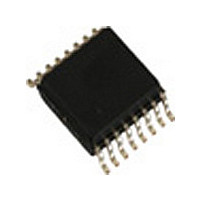
CY2DP814ZC Cypress Semiconductor Corp, CY2DP814ZC Datasheet - Page 3

CY2DP814ZC
Manufacturer Part Number
CY2DP814ZC
Description
Manufacturer
Cypress Semiconductor Corp
Datasheet
1.CY2DP814ZC.pdf
(9 pages)
Specifications of CY2DP814ZC
Number Of Outputs
8
Operating Supply Voltage (max)
3.465V
Operating Temp Range
0C to 70C
Propagation Delay Time
<4ns
Operating Supply Voltage (min)
3.135V
Mounting
Surface Mount
Pin Count
16
Operating Supply Voltage (typ)
3.3V
Package Type
TSSOP
Power Dissipation
750W
Input Frequency
450MHz
Operating Temperature Classification
Commercial
Lead Free Status / Rohs Status
Not Compliant
Available stocks
Company
Part Number
Manufacturer
Quantity
Price
Company:
Part Number:
CY2DP814ZC
Manufacturer:
SUN
Quantity:
103
Part Number:
CY2DP814ZC
Manufacturer:
CYPRESS/赛普拉斯
Quantity:
20 000
Maximum Ratings
Storage Temperature: ................................. –65C to +150C
Ambient Temperature: .................................. –40C to +85C
Supply Voltage to Ground Potential
(Inputs and V
Table 1. EN1 EN2 Function Table
Table 2. Input Receiver Configuration for Differential or LVTTL/LVCMOS
Table 3. Function Control of the TTL Input Logic Used to Accept or Invert the Input Signal
Table 4. Power Supply Characteristics
Table 5. DC Electrical Characteristics: 3.3V–LVDS Input
Document Number: 38-07060 Rev. *F
I
I
V
V
I
I
I
Notes
Parameter
Parameter
CCD
C
IH
IL
I
CONFIG Pin 2 Binary Value
1. Stresses greater than those listed under absolute maximum ratings may cause permanent damage to the device. This is intended to be a stress rating only and
2. Multiple Supplies: The voltage on any input or I/O pin cannot exceed the power pin during power-up. Power supply sequencing is NOT required.
ID
IC
Ground
Ground
functional operation of the device at these or any other conditions above those indicated in the operation sections of this specification is not implied. Exposure
to absolute maximum rating conditions for extended periods may affect reliability.
V
V
CC
CC
EN1
H
H
L
L
Dynamic Power Supply Current V
Total Power Supply Current
CC
Magnitude of Differential Input Voltage
Common-Mode of Differential Input Voltage
IV
Input High Current
Input Low Current
Input High Current
Enable Logic
Input Condition
1
0
ID
only) .......................................–0.3V to 4.6V
I (min. and max.)
Description
IN+ Pin 6
IN+ Pin 6
IN+ Pin 6
IN+ Pin 6
IN– Pin 7
IN– Pin 7
IN– Pin 7
IN– Pin 7
[1, 2]
Description
EN2
H
H
L
L
LVTTL in LVCMOS
LVDS
LVPECL
Input Receiver Family
Input toggling 50% Duty Cycle, Outputs Loaded
V
Input toggling 50% Duty Cycle, Outputs Loaded,
fL= 100 MHz
DD
DD
LVTTL/LVCMOS INPUT LOGIC
= Max.
= Max.
IN+
H
H
H
X
Input Logic
Input
Input
Input
Input
V
V
V
DD
DD
DD
Single ended, non-inverting, inverting, void of bias resistors.
Low voltage differential signaling
Low voltage pseudo (positive) emitter coupled logic
Input
Test Conditions
= Max.
= Max.
= Max., V
Supply Voltage to Ground Potential
(Outputs only) ........................................ –0.3V to V
DC Input Voltage ................................... –0.3V to V
DC Output Voltage................................. –0.3V to V
Power Dissipation........................................................ 0.75W
IN–
IN
X
L
L
L
Conditions
= V
DD
(max.)
Input Receiver Type
Output Logic Q pins
V
V
IN
IN
QnA
= V
= V
H
H
H
Z
Min
DD
SS
Invert
Invert
True
True
Outputs
IV
Min
100
Typ
1.5
/2
90
ID
I
Typ Max Unit
±10 ±20
(IV
±0
Max
100
2.0 mA/MHz
2.4–
CY2DP814
ID
QnB
I /2)
Z
L
L
L
600 mV
±20
±20
DD
DD
DD
Unit
mA
Page 3 of 9
+ 0.3V
+ 0.3V
+ 0.9V
A
A
A
V
[+] Feedback
[+] Feedback


