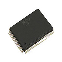
CY7C1370C-167AI Cypress Semiconductor Corp, CY7C1370C-167AI Datasheet - Page 19

CY7C1370C-167AI
Manufacturer Part Number
CY7C1370C-167AI
Description
Manufacturer
Cypress Semiconductor Corp
Datasheet
1.CY7C1370C-167AI.pdf
(27 pages)
Specifications of CY7C1370C-167AI
Density
18Mb
Access Time (max)
3.4ns
Sync/async
Synchronous
Architecture
SDR
Clock Freq (max)
166MHz
Operating Supply Voltage (typ)
3.3V
Address Bus
19b
Package Type
TQFP
Operating Temp Range
-40C to 85C
Number Of Ports
1
Supply Current
275mA
Operating Supply Voltage (min)
3.135V
Operating Supply Voltage (max)
3.465V
Operating Temperature Classification
Industrial
Mounting
Surface Mount
Pin Count
100
Word Size
36b
Number Of Words
512K
Lead Free Status / Rohs Status
Not Compliant
Available stocks
Company
Part Number
Manufacturer
Quantity
Price
Part Number:
CY7C1370C-167AI
Manufacturer:
CYPRESS/赛普拉斯
Quantity:
20 000
Document #: 38-05233 Rev. *D
Capacitance
Thermal Resistance
Switching Characteristics
C
C
C
AC Test Loads and Waveforms
t
Clock
t
F
t
t
Output Times
t
t
t
t
t
t
t
Shaded areas contain advance information.
Notes:
16. Tested initially and after any design or process changes that may affect these parameters.
17. This part has a voltage regulator internally; tpower is the time power needs to be supplied above Vdd minimum initially, before a Read or Write operation can be
18. t
19. At any given voltage and temperature, t
20. This parameter is sampled and not 100% tested.
21. Timing reference is 1.5V when V
22. Test conditions shown in (a) of AC Test Loads unless otherwise noted.
Power
CYC
CH
CL
CO
EOV
DOH
CHZ
CLZ
EOHZ
EOLZ
Parameters
MAX
Parameter
IN
CLK
I/O
OUTPUT
Parameter
initiated.
data bus. These specifications do not imply a bus contention condition, but reflect parameters guaranteed over worst case user conditions. Device is designed
to achieve High-Z prior to Low-Z under the same system conditions.
CHZ
Q
Q
[17]
, t
JA
JC
CLZ
, t
EOLZ
Thermal Resistance
(Junction to Ambient)
Thermal Resistance
(Junction to Case)
Input Capacitance
Clock Input Capacitance
Input/Output Capacitance
[16]
, and t
Z
V
Clock Cycle Time
Maximum Operating Frequency
Clock HIGH
Clock LOW
Data Output Valid After CLK Rise
OE LOW to Output Valid
Data Output Hold After CLK Rise
Clock to High-Z
Clock to Low-Z
OE HIGH to Output High-Z
OE LOW to Output Low-Z
0
CC
= 50Ω
Description
EOHZ
(typical) to the first access read or write
(a)
Description
are specified with AC test conditions shown in (b) of AC Test Loads. Transition is measured ± 200 mV from steady-state voltage.
[16]
V
L
= 1.25V
DDQ=
[18, 19, 20]
Description
[18, 19, 20]
R
3.3V and is 1.25V when V
L
EOHZ
Over the Operating Range
= 50Ω
is less than t
Test conditions follow
standard test methods and
procedures for measuring
thermal impedance, per EIA
/ JESD51.
[18, 19, 20]
[18, 19, 20]
Output
T
V
2.5V
INCLUDING
Test Conditions
A
DD
EOLZ
JIG AND
= 25°C, f = 1 MHz,
SCOPE
Test Conditions
= 2.5V V
and t
5 pF
DDQ=
CHZ
2.5V.
DDQ
is less than t
(b)
[ 21, 22]
Min. Max. Min. Max. Min. Max. Min. Max.
4.0
1.7
1.7
1.0
1.0
= 2.5V
R=1667Ω
1
0
-250
R = 1538Ω
CLZ
250
2.6
2.6
2.6
2.6
BGA Typ.
to eliminate bus contention between SRAMs when sharing the same
45
BGA Max.
7
V
0V
4.4
2.0
2.0
1.0
1.0
DD
1
0
8
8
8
-225
< 1.0 ns
225
fBGA Typ.
2.8
2.8
2.8
2.8
10%
90%
46
3
fBGA Max.
2.0
2.0
1.3
1.3
ALL INPUT PULSES
1
5
0
-200
9
9
9
1.25V
TQFP Typ.
200
3.0
3.0
3.0
3.0
(c)
31
6
TQFP Max.
2.2
2.2
1.3
1.3
CY7C1370C
CY7C1372C
1
6
0
-167
5
5
5
[16]
°C/W
°C/W
166
90%
Unit
3.4
3.4
3.4
3.4
Page 19 of 27
10%
< 1.0 ns
Notes
MHz
Unit
Unit
ms
ns
ns
ns
ns
ns
ns
ns
ns
ns
ns
pF
pF
pF
17
17
[+] Feedback


