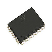
CY7C1360B-200AC Cypress Semiconductor Corp, CY7C1360B-200AC Datasheet - Page 14

CY7C1360B-200AC
Manufacturer Part Number
CY7C1360B-200AC
Description
Manufacturer
Cypress Semiconductor Corp
Datasheet
1.CY7C1360B-200AC.pdf
(34 pages)
Specifications of CY7C1360B-200AC
Density
9Mb
Access Time (max)
3ns
Sync/async
Synchronous
Architecture
SDR
Clock Freq (max)
200MHz
Operating Supply Voltage (typ)
3.3V
Address Bus
18b
Package Type
TQFP
Operating Temp Range
0C to 70C
Number Of Ports
1
Supply Current
220mA
Operating Supply Voltage (min)
3.135V
Operating Supply Voltage (max)
3.465V
Operating Temperature Classification
Commercial
Mounting
Surface Mount
Pin Count
100
Word Size
36b
Number Of Words
256K
Lead Free Status / Rohs Status
Not Compliant
Document #: 38-05291 Rev. *C
Truth Table
Deselect Cycle, Power Down
Deselect Cycle, Power Down
Deselect Cycle, Power Down
Deselect Cycle, Power Down
Deselect Cycle, Power Down
Snooze Mode, Power Down
READ Cycle, Begin Burst
READ Cycle, Begin Burst
WRITE Cycle, Begin Burst
READ Cycle, Begin Burst
READ Cycle, Begin Burst
READ Cycle, Continue Burst
READ Cycle, Continue Burst
READ Cycle, Continue Burst
READ Cycle, Continue Burst
WRITE Cycle, Continue Burst
WRITE Cycle, Continue Burst
READ Cycle, Suspend Burst
READ Cycle, Suspend Burst
READ Cycle, Suspend Burst
READ Cycle, Suspend Burst
WRITE Cycle, Suspend Burst
WRITE Cycle, Suspend Burst
Notes:
3. X = “Don't Care.” H = Logic HIGH, L = Logic LOW.
4. WRITE = L when any one or more Byte Write Enable signals and BWE = L or GW = L. WRITE = H when all Byte Write Enable signals, BWE, GW = H.
5. The DQ pins are controlled by the current cycle and the OE signal. OE is asynchronous and is not sampled with the clock.
6. CE
7. The SRAM always initiates a read cycle when ADSP is asserted, regardless of the state of GW, BWE, or BW
8. OE is asynchronous and is not sampled with the clock rise. It is masked internally during Write cycles. During a Read cycle all data bits are Three-State when
9. Table only lists a partial listing of the byte write combinations. Any combination of BW
after the ADSP or with the assertion of ADSC . As a result, OE must be driven HIGH prior to the start of the Write cycle to allow the outputs to three-state. OE is
a don't care for the remainder of the Write cycle
OE is inactive or when the device is deselected, and all data bits behave as output when OE is active (LOW) .
1
, CE
2
Operation
, and CE
[3, 4, 5, 6, 7, 8]
3
are available only in the TQFP package. BGA package has only 2 chip selects CE
Add. Used CE
External
External
External
External
External
Current
Current
Current
Current
Current
Current
None
None
None
None
None
None
Next
Next
Next
Next
Next
Next
H
H
H
H
H
H
H
X
L
L
X
X
X
X
X
X
L
L
L
L
L
L
L
1
CE
H
H
H
H
H
X
X
X
X
X
X
X
X
X
X
X
X
X
X
X
X
L
L
2
CE
X
X
H
X
H
X
X
X
X
X
X
X
X
X
X
X
X
X
L
L
L
L
L
3
ZZ ADSP ADSC ADV WRITE OE CLK
H
L
L
L
L
L
L
L
L
L
L
L
L
L
L
L
L
L
L
L
L
L
L
[A:D]
is valid. Appropriate write will be done based on which byte write is active.
H
X
H
H
X
H
H
H
H
X
X
H
X
H
H
X
X
H
X
L
L
L
L
X
X
X
H
H
H
H
H
H
H
H
H
H
H
H
L
X
X
L
L
L
L
L
1
and CE
X
H
H
H
H
H
H
X
X
X
X
X
X
X
X
X
X
X
L
L
L
L
L
L
. Writes may occur only on subsequent clocks
2
.
X
X
X
X
X
X
X
X
H
H
H
H
H
H
H
H
H
H
L
L
L
L
L
X
X
X
X
X
X
H
X
H
H
H
X
X
H
H
X
X
L
L
L
L
L
L
CY7C1360B
CY7C1362B
L-H Three-State
L-H Three-State
L-H Three-State
L-H Three-State
L-H Three-State
L-H
L-H Three-State
L-H
L-H
L-H Three-State
L-H
L-H Three-State
L-H
L-H Three-State
L-H
L-H
L-H
L-H Three-State
L-H
L-H Three-State
L-H
L-H
X
Page 14 of 34
Three-State
DQ
Q
D
Q
Q
Q
D
D
Q
Q
D
D


