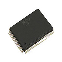
CY7C1360B-200AC Cypress Semiconductor Corp, CY7C1360B-200AC Datasheet - Page 11

CY7C1360B-200AC
Manufacturer Part Number
CY7C1360B-200AC
Description
Manufacturer
Cypress Semiconductor Corp
Datasheet
1.CY7C1360B-200AC.pdf
(34 pages)
Specifications of CY7C1360B-200AC
Density
9Mb
Access Time (max)
3ns
Sync/async
Synchronous
Architecture
SDR
Clock Freq (max)
200MHz
Operating Supply Voltage (typ)
3.3V
Address Bus
18b
Package Type
TQFP
Operating Temp Range
0C to 70C
Number Of Ports
1
Supply Current
220mA
Operating Supply Voltage (min)
3.135V
Operating Supply Voltage (max)
3.465V
Operating Temperature Classification
Commercial
Mounting
Surface Mount
Pin Count
100
Word Size
36b
Number Of Words
256K
Lead Free Status / Rohs Status
Not Compliant
Document #: 38-05291 Rev. *C
CY7C1362B–Pin Definitions
V
MODE
TDO
TDI
TMS
TCK
NC
DDQ
Name
4,11,20,27,
54,61,70,
1,2,3,6,7,
14,16,25,
28,29,30,
38,39,42,
51,52,53,
56,57,66,
75,78,79,
Enable
3-Chip
TQFP
95,96
77
31
-
-
-
-
4,11,20,27,
54,61,70,
1,2,3,6,7,
14,16,25,
28,29,30,
38,39,42,
43,51,52,
53,56,57,
66,75,78,
79,95,96
Enable
2-Chip
TQFP
77
31
-
-
-
-
A1,A7,F1,
N2,L7,P1,
K6,L4,L2,
J3,J5,K1,
T1,T4,U6
F7,J1,J7,
(continued)
M1,M7,
C1,C7,
D2,D4,
G6,H7,
R5,R7,
B1,B7,
D7,E1,
E6,H2,
F2,G1,
L7,M6,
P6,R1,
U1,U7
BGA
R3
U5
U3
U2
U4
C1,C2,C10,
G10,H1,H3,
N2,N7,N10,
N5,N11,P1,
E1,E10,F1,
H9,H10,J2,
A1,B11,P2,
C3,C9,D3,
L9,M3,M9,
K11,L2,L1,
D9,E3,E9,
F3,F9,G3,
A5,B1,B4,
G9,J3,J9,
K3,K9,L3,
M2,M11,
D1,D10,
F10,G1,
J11,K2,
N3,N9
R2,N6
fBGA
R1
P7
P5
R5
R7
Synchronous
Synchronous
Synchronous
JTAG-Clock Clock input to the JTAG circuitry. If the JTAG
JTAG serial
JTAG serial
JTAG serial
I/O Power
Supply
output
Input-
Static
input
input
I/O
-
Power supply for the I/O circuitry.
Selects Burst Order. When tied to GND selects
linear burst sequence. When tied to V
floating selects interleaved burst sequence. This is
a strap pin and should remain static during device
operation. Mode pin has an internal pull-up.
Serial data-out to the JTAG circuit. Delivers data
on the negative edge of TCK. If the JTAG feature
is not being utilized, this pin should be left uncon-
nected. This pin is not available on TQFP
packages.
Serial data-In to the JTAG circuit. Sampled on
the rising edge of TCK. If the JTAG feature is not
being utilized, this pin can be left floating or con-
nected to V
is not available on TQFP packages.
Serial data-In to the JTAG circuit. Sampled on
the rising edge of TCK. If the JTAG feature is not
being utilized, this pin can be disconnected or con-
nected to V
packages.
feature is not being utilized, this pin must be
connected to V
TQFP packages.
No Connects. Not internally connected to the die.
DD
DD
. This pin is not available on TQFP
through a pull-up resistor. This pin
SS
. This pin is not available on
Description
CY7C1360B
CY7C1362B
Page 11 of 34
DD
or left


