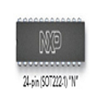
S87C751-4N24 NXP Semiconductors, S87C751-4N24 Datasheet - Page 6

S87C751-4N24
Manufacturer Part Number
S87C751-4N24
Description
Manufacturer
NXP Semiconductors
Datasheet
1.S87C751-4N24.pdf
(24 pages)
Specifications of S87C751-4N24
Cpu Family
87C
Device Core
80C51
Device Core Size
8b
Frequency (max)
16MHz
Interface Type
I2C/UART
Program Memory Type
EPROM
Program Memory Size
2KB
Total Internal Ram Size
64Byte
# I/os (max)
19
Number Of Timers - General Purpose
1
Operating Supply Voltage (typ)
5V
Operating Supply Voltage (max)
5.5V
Operating Supply Voltage (min)
4.5V
Instruction Set Architecture
CISC
Operating Temp Range
0C to 70C
Operating Temperature Classification
Commercial
Mounting
Through Hole
Pin Count
24
Package Type
PDIP
Lead Free Status / Rohs Status
Not Compliant
1. Stresses above those listed under Absolute Maximum Ratings may cause permanent damage to the device. This is a stress rating only and
2. This product includes circuitry specifically designed for the protection of its internal devices from the damaging effects of excessive static
Philips Semiconductors
ABSOLUTE MAXIMUM RATINGS
NOTES:
DC ELECTRICAL CHARACTERISTICS
T
NOTES TO DC ELECTRICAL CHARACTERISTICS ON NEXT PAGE.
1998 May 01
amb
SYMBOL
SYMBOL
V
V
V
V
V
V
V
V
V
C
I
I
I
R
C
I
V
I
I
IL
TL
LI
PD
PP
CC
IL
IH
IH1
IL1
IH2
OL
OL1
OH
OL2
PP
80C51 8-bit microcontroller family
2K/64 OTP/ROM, I
Storage temperature range
Voltage from V
Voltage from any pin to V
Power dissipation
Voltage on V
Maximum I
RST
IO
functional operation of the device at these or any conditions other than those described in the AC and DC Electrical Characteristics section
of this specification is not implied.
charge. Nonetheless, it is suggested that conventional precautions be taken to avoid applying greater than the rated maxima.
= 0 C to +70 C or –40 C to +85 C, V
OL
PP
Input low voltage, except SDA, SCL
Input high voltage, except X1, RST
Input high voltage, X1, RST
SDA, SCL, P0.2
Input low voltage
Input high voltage
Output low voltage, ports 1 and 3
Output low voltage, port 0.2
Output high voltage, ports 1 and 3
Port 0.0 and 0.1 (I
Output low voltage
Driver, receiver combined:
Capacitance
Logical 0 input current, ports 1 and 3
Logical 1 to 0 transition current, ports 1 and 3
Input leakage current, port 0
Internal pull-down resistor
Pin capacitance
Power-down current
V
Program current (for 87C751 only)
Supply current (see Figure 2)
per I/O pin
PP
CC
pin to V
program voltage (for 87C751 only)
to V
SS
SS
SS
(except V
2
C) – Drivers
PARAMETER
PARAMETER
4
2
C, low pin count
PP
CC
)
1, 2
PARAMETER
= 5V 10% for 87C751, V
3
CC
6
V
= 5V 10% for 83C751, V
IN
TEST CONDITIONS
TEST CONDITIONS
T
V
V
amb
Test freq = 1MHz,
(over V
IN
CC
0.45 < V
= 2V (–40 to +85 C)
V
I
I
I
I
I
= 2V (0 to 70 C)
T
V
CC
OL
OL
V
OH
OH
OH
= 2 to V
I
amb
= 21 C to 27 C
PP
OL
V
IN
SS
= 1.6mA
= 3.2mA
= 5V 10%
= –60 A
= –25 A
= –10 A
= 0.45V
= 13.0V
= 3mA
CC
= 25 C
IN
= 0V
range)
< V
CC
2
2
CC
max
SS
0.2V
= 0V
0.75V
0.7V
0.7V
0.9V
MIN
–0.5
–0.5
12.5
2.4
CC
25
–0.5 to V
1
CC
CC
CC
+0.9
CC
–65 to +150
–0.5 to +6.5
0 to +13.0
LIMITS
RATING
83C751/87C751
1.0
10
CC
0.2V
V
V
V
0.3V
CC
CC
CC
+ 0.5
MAX
–650
–750
0.45
0.45
13.0
–50
175
0.4
DD
10
10
50
50
10
+0.5
+0.5
+0.5
Product specification
CC
–0.1
UNIT
UNIT
UNIT
mA
mA
pF
k
pF
W
V
V
V
V
V
V
V
V
V
V
V
V
V
V
V
C
A
A
A
A
A


