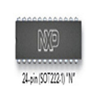
S87C751-4N24 NXP Semiconductors, S87C751-4N24 Datasheet - Page 5

S87C751-4N24
Manufacturer Part Number
S87C751-4N24
Description
Manufacturer
NXP Semiconductors
Datasheet
1.S87C751-4N24.pdf
(24 pages)
Specifications of S87C751-4N24
Cpu Family
87C
Device Core
80C51
Device Core Size
8b
Frequency (max)
16MHz
Interface Type
I2C/UART
Program Memory Type
EPROM
Program Memory Size
2KB
Total Internal Ram Size
64Byte
# I/os (max)
19
Number Of Timers - General Purpose
1
Operating Supply Voltage (typ)
5V
Operating Supply Voltage (max)
5.5V
Operating Supply Voltage (min)
4.5V
Instruction Set Architecture
CISC
Operating Temp Range
0C to 70C
Operating Temperature Classification
Commercial
Mounting
Through Hole
Pin Count
24
Package Type
PDIP
Lead Free Status / Rohs Status
Not Compliant
1. When P0.2 is at or close to 0V it may affect the internal ROM operation. We recommend that P0.2 be tied to V
Philips Semiconductors
PIN DESCRIPTIONS
NOTE:
1998 May 01
MNEMONIC
V
V
P0.0–P0.2
P1.0–P1.7
P3.0–P3.7
RST
X1
X2
SS
CC
80C51 8-bit microcontroller family
2K/64 OTP/ROM, I
(e.g., 2k ).
SSOP
13–20
23–21
DIP/
5–1,
8–6
12
24
18
19
20
10
11
6
7
8
7
8
9
PIN NO.
15–20,
6, 4–1,
23, 24
27–25
LCC
9–7
14
28
20
23
24
13
12
11
7
8
9
8
9
TYPE
N/A
2
I/O
I/O
I/O
I/O
I/O
O
I
I
I
I
I
I
I
I
I
C, low pin count
Circuit Ground Potential
Supply voltage during normal, idle, and power-down operation.
Port 0: Port 0 is a 3-bit open-drain, bidirectional port. Port 0 pins that have 1s written to them float,
and in that state can be used as high-impedance inputs. Port 0 also serves as the serial I
interface. When this feature is activated by software, SCL and SDA are driven low in accordance
with the I
subsystem presents a 0. The state of the pin can always be read from the port register by the
program.
To comply with the I
electrical characteristics listed in the tables that follow. While these differ from “standard TTL”
characteristics, they are close enough for the pins to still be used as general-purpose I/O in
non-I
memory as follows:
V
OE/PGM (P0.1) – Input which specifies verify mode (output enable) or the program mode.
OE/PGM = 1 output enabled (verify mode).
OE/PGM = 0 program mode.
ASEL (P0.0) – Input which indicates which bits of the EPROM address are applied to port 3.
ASEL = 0 low address byte available on port 3.
ASEL = 1 high address byte available on port 3 (only the three least significant bits are used).
SDA (P0.1) – I
SCL (P0.0) – I
Port 1: Port 1 is an 8-bit bidirectional I/O port with internal pull-ups. Port 1 pins that have 1s written
to them are pulled high by the internal pull-ups and can be used as inputs. As inputs, port 1 pins
that are externally pulled low will source current because of the internal pull-ups. (See DC
Electrical Characteristics: I
mode and accepts as inputs the value to program into the selected address during the program
mode. Port 1 also serves the special function features of the 80C51 family as listed below:
INT0 (P1.5): External interrupt.
INT1 (P1.6): External interrupt.
T0 (P1.7): Timer 0 external input.
Port 3: Port 3 is an 8-bit bidirectional I/O port with internal pull-ups. Port 3 pins that have 1s written
to them are pulled high by the internal pull-ups and can be used as inputs. As inputs, port 3 pins
that are externally being pulled low will source current because of the pull-ups. (See DC Electrical
Characteristics: I
be programmed (or verified). The 11-bit address is multiplexed into this port as specified by
P0.0/ASEL.
Reset: A high on this pin for two machine cycles while the oscillator is running, resets the device.
An internal diffused resistor to V
V
the device in the programming state allowing programming address, data and V
programming or verification purposes. The RESET serial sequence must be synchronized with the
X1 input.
Crystal 1: Input to the inverting oscillator amplifier and input to the internal clock generator circuits.
X1 also serves as the clock to strobe in a serial bit stream into RESET to place the device in the
programming state.
Crystal 2: Output from the inverting oscillator amplifier.
PP
CC
. After the device is reset, a 10-bit serial sequence, sent LSB first, applied to RESET, places
(P0.2) – Programming voltage input. (See Note 1.)
2
C applications. Port 0 also provides alternate functions for programming the EPROM
2
C protocol. These pins are driven low if the port register bit is written with a 0 or if the I
2
2
C clock.
C data.
IL
). Port 3 also functions as the address input for the EPROM memory location to
2
C specification, P0.0 and P0.1 are open drain bidirectional I/O pins with the
IL
). Port 1 serves to output the addressed EPROM contents in the verify
5
SS
permits a power-on RESET using only an external capacitor to
NAME AND FUNCTION
83C751/87C751
CC
via a small pullup
PP
Product specification
to be applied for
2
C
2
C


