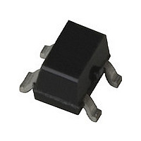
MSA-2643-BLK Avago Technologies US Inc., MSA-2643-BLK Datasheet - Page 9

MSA-2643-BLK
Manufacturer Part Number
MSA-2643-BLK
Description
Manufacturer
Avago Technologies US Inc.
Datasheet
1.MSA-2643-BLK.pdf
(15 pages)
Specifications of MSA-2643-BLK
Manufacturer's Type
MMIC Amplifier
Number Of Channels
1
Supply Current
70mA
Frequency (max)
6GHz
Operating Supply Voltage (min)
3V
Operating Supply Voltage (typ)
3.4V
Operating Supply Voltage (max)
3.8V
Package Type
SOT-343
Mounting
Surface Mount
Pin Count
3 +Tab
Noise Figure (typ)
3.6@2000MHzdB
Lead Free Status / Rohs Status
Not Compliant
9
MSA-2643 RFIC Amplifier
Description
Avago Technologies’ MSA-2643
is a low current silicon gain
block RFIC amplifier housed in
a 4-lead SC-70 (SOT-343) surface
mount plastic package. Provid-
ing a nominal 16.9 dB gain at up
to +14.5 dBm Pout, this device is
ideal for small-signal gain stages
or IF amplification. The Darlington
feedback structure provides inher-
ent broad bandwidth performance.
The 25 GHz f
results in a device with low cur-
rent draw and useful operation
above 3 GHz.
A feature of the MSA-2643 is its
broad bandwidth that is useful in
many satellite-based TV, cable TV
and datacom systems.
In addition to use in buffer and
driver amplifier applications in
the TV market, the MSA-2643 will
find many applications in wireless
communication systems.
Application Guidelines
The MSA-2643 is very easy to use.
For most applications, all that is
required to operate the MSA-2643
is to apply 27 mA to 45 mA to the
RF Output pin.
RF Input and Output
The RF Input and Output ports
of the MSA-25643 are closely
matched to 50Ω.
DC Bias
The MSA-2643 is a current-biased
device that operates from a 27 mA
to 45 mA current source. Curves
of typical performance as a func-
tion of bias current are shown
in section one of the data sheet.
Figure 1 shows a typical imple-
mentation of the MSA-2643. The
supply current for the MSA-2643
must be applied to the RF Output
pin. The power supply connection
t
fabrication process
to the RF Output pin is achieved
by means of a RF choke (induc-
tor). The value of the RF choke
must be large relative to 50Ω in
order to prevent loading of the RF
Output. The supply voltage end
of Rc is bypassed to ground with
a capacitor. Blocking capacitors
are normally placed in series with
the RF Input and the RF Output to
isolate the DC voltages on these
pins from circuits adjacent to the
amplifier. The values for the block-
ing and bypass capacitors are
selected to provide a reactance at
the lowest frequency of operation
that is small relative to 50Ω.
Figure 1. Schematic Diagram with Bias
Connections.
PCB Layout
A recommended PCB pad layout
for the miniature SOT-343 (SC-
70) package that is used by the
MSA-2643 is shown in Figure 2.
0.031
Figure 2. PCB Pad Layout for MSA-2643.
Package dimensions in mm/inches.
This layout provides ample allow-
ance for package placement by
automated assembly equipment
without adding parasitics that
could impair the high frequency
RF performance of the MSA-
0.80
C1
0.020
0.50
26x
0.045
1.15
0.051
V
1.30
d
RFC
Rc
C2
C3
0.067
0.031
1.71
.080
Vcc
2643. The layout is shown with a
footprint of a SOT-343 package
superimposed on the PCB pads for
reference.
Starting with the package pad
layout in Figure 3, an RF layout
similar to the one shown in Fig-
ure 3 is a good starting point for
microstripline designs using the
MSA-2643 amplifier.
PCB Materials
FR-4 or G-10 type materials are
good choices for most low cost
wireless applications using single
or multi-layer printed circuit
boards. Typical single-layer board
thickness is 0.020 to 0.031 inches.
Circuit boards thicker than 0.031
inches are not recommended due
to excessive inductance in the
ground vias. This is discussed in
more detail in the section on RF
grounding.
Applications Example
The printed circuit layout in Fig-
ure 3 is a multi-purpose layout that
will accommodate components for
using the MSA-2643 for RF inputs
from DC through 3 GHz. This
layout is a microstripline design
(solid groundplane on the back-
side of the circuit board) with 50Ω
interfaces for the RF input and
output. The circuit is fabricated
on 0.031-inch thick FR-4 dielectric
material. Plated through holes
(vias) are used to bring the ground
to the top side of the circuit where
needed. Multiple vias are used to
reduce the inductance of the paths
to ground.


