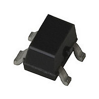
MSA-2643-BLK Avago Technologies US Inc., MSA-2643-BLK Datasheet - Page 10

MSA-2643-BLK
Manufacturer Part Number
MSA-2643-BLK
Description
Manufacturer
Avago Technologies US Inc.
Datasheet
1.MSA-2643-BLK.pdf
(15 pages)
Specifications of MSA-2643-BLK
Manufacturer's Type
MMIC Amplifier
Number Of Channels
1
Supply Current
70mA
Frequency (max)
6GHz
Operating Supply Voltage (min)
3V
Operating Supply Voltage (typ)
3.4V
Operating Supply Voltage (max)
3.8V
Package Type
SOT-343
Mounting
Surface Mount
Pin Count
3 +Tab
Noise Figure (typ)
3.6@2000MHzdB
Lead Free Status / Rohs Status
Not Compliant
10
Figure 3. Multi-purpose Evaluation Board.
The amplifier and related com-
ponents are assembled onto the
printed circuit board as shown in
Figure 6. The MSA-2X43 circuit
board is designed to use edge-
mounting SMA connectors such as
Johnson Components, Inc., Model
142-0701-881. These connectors
are designed to slip over the edge
of 0.031-inch thick circuit boards
and obviate the need to mount
PCBs on a metal base plate for
testing. The center conductors of
the connectors are soldered to the
input and output microstrip lines.
The ground pins are soldered to
the ground plane on the back of
the board and to the top ground
pads.
DC blocking capacitors are re-
quired at the input and output of
the IC. The values of the blocking
capacitors are determined by the
lowest frequency of operation
for a particular application. The
capacitor’s reactance is chosen to
be 10% or less of the amplifier’s
input or output impedance at the
lowest operating frequency. For
example, an amplifier to be used
in an application covering the
900 MHz band would require an
input blocking capacitor of at least
39 pF, which is 4.5Ω of reactance
at 900 MHz. The Vcc connection to
the amplifier must be RF bypassed
by placing a capacitor to ground at
the bias pad of the board. Like the
DC blocking capacitors, the value
of the Vcc bypass capacitor is
Agilent Technologies
MSA-2X43
IN
OUT
IP 4/00
Vcc
determined by the lowest operat-
ing frequency for the amplifier.
Space is available on the circuit
board to add a bias choke, bypass
capacitors, and collector resistors.
The MSA series of ICs requires
a bias resistor to ensure thermal
stability. The bias resistor value
is calculated from the operating
current value, device voltage and
the supply voltage; see equation
below. When applying bias to the
board, start at a low voltage level
and slowly increase the voltage
until the recommended current is
reached. Both power and gain can
be adjusted by varying I
Rc = Vcc – V
Where:
Vcc = The power supply voltage
V
I
Notes on Rc Selection
The value of Rc is dependant on
V
will have an effect on I
gain and power performance of
the MSA-2643 may be adjusted
by varying I
taken into account. The char-
Table 1. Effects of Rc on Performance over Temperature.
Operating voltage = 3.4V nominally.
Voltage
Drop, volts
0
1.5
4.0
6.5
d
d
d
=
, any production variation in V
=
applied to Rc (volts)
The device voltage (volts)
The quiescent bias current
drawn by the device
I
d
d
d
this will have to be
Resistor
Value, Ohms
0
56
150
40
Ω
d
. As the
d
.
Temperature,
°C
0
5
85
0
5
85
0
5
85
0
5
85
d
acterization data in section one
shows the relationship between
V
lower temperatures the value
of V
in V
production variations may cause
potential problems for the am-
plifier performance if it is not
taken into account. One solution
would be to increase the voltage
supply to have at least a 4V drop
across the bias resistor Rc. This
will guarantee good temperature
stability over temperature. Table
1 shows the effects of Rc on the
performance of the MSA-2643 over
temperature.
An alternative solution to ensure
good temperature stability with-
out having a large voltage drop
across a resistor would be to use
an active bias circuit as shown
in Figure 4. The resistors R1 and
the PNP transistor connected to
form a diode by connecting the
base and collector together and R2
form a potential diver circuit to set
the base voltage of the bias PNP
transistor. The diode connected
PNP transistor is used to com-
pensate for the voltage variation
with temperature of the bias PNP
transistor. R3 provides a bleed
path for any excess bias; it is a
safety feature and can be omitted
d
and I
d
d
at low temperatures and
increases. The increase
Bias Current,
mA
16.7
7.0
40.7
5.4
7.0
30.5
6.
7.0
8.5
6.5
7.0
8.0
d
over temperature. At
Power Gain @
2.0 GHz, dB
14.8
15.4
15.3
15.6
15.4
15.0
15.6
15.4
15.1
15.6
15.4
15.1


