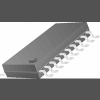
LMX2332LTM National Semiconductor, LMX2332LTM Datasheet - Page 21

LMX2332LTM
Manufacturer Part Number
LMX2332LTM
Description
83F3835
Manufacturer
National Semiconductor
Datasheet
1.LMX2332LTM.pdf
(26 pages)
Specifications of LMX2332LTM
Pll Type
Frequency Synthesis
Frequency
1.1GHz
Supply Current
3mA
Supply Voltage Range
2.7V To 5.5V
Digital Ic Case Style
TSSOP
No. Of Pins
20
Operating Temperature Range
-40°C To +85°C
Rohs Compliant
No
Available stocks
Company
Part Number
Manufacturer
Quantity
Price
Company:
Part Number:
LMX2332LTM
Manufacturer:
NS
Quantity:
8 056
Part Number:
LMX2332LTM
Manufacturer:
NS/国半
Quantity:
20 000
Part Number:
LMX2332LTME
Manufacturer:
NS/国半
Quantity:
20 000
Company:
Part Number:
LMX2332LTMG
Manufacturer:
NS
Quantity:
21
Part Number:
LMX2332LTMG
Manufacturer:
NS/国半
Quantity:
20 000
Company:
Part Number:
LMX2332LTMX
Manufacturer:
NS/TI
Quantity:
3 500
relationships. To maintain the same gain/phase relationship
at twice the original cutoff frequency, other terms in the gain
and phase
sate by the corresponding “1/w” or “1/w
of equations Equations 2, 3 and
damping resistor variable R2 could be chosen to compensate
the “w”' terms for the phase margin. This implies that another
resistor of equal value to R2 will need to be switched in par-
allel with R2 during the initial lock period. We must also insure
FASTLOCK CIRCUIT IMPLEMENTATION
A diagram of the Fastlock scheme as implemented in National
Semiconductors LMX233XL PLL is shown in
a new frequency is loaded, and the RF Icp
charge pump circuit receives an input to deliver 4 times the
normal current per unit phase error while an open drain
NMOS on chip device switches in a second R2 resistor ele-
ment to ground. The user calculates the loop filter component
values for the normal steady state considerations. The device
configuration ensures that as long as a second identical
Equation 4
and
Equation 5
Equation 5
12806 Version 9 Revision 2
2
will have to compen-
” factor. Examination
FIGURE 4. Open Loop Response Bode Plot
o
bit is set high the
FIGURE 5. Fastlock PLL Architecture
Figure
indicates the
5. When
Print Date/Time: 2011/07/11 15:54:42
21
that the magnitude of the open loop gain, H(s)G(s) is equal to
zero at wp' = 2wp. K
terms can be changed by a factor of 4, to counteract the w
term present in the denominator of
3. The Kφ term was chosen to complete the transformation
because it can readily be switched between 1X and 4X val-
ues. This is accomplished by increasing the charge pump
output current from 1 mA in the standard mode to 4 mA in
Fastlock.
damping resistor is wired in appropriately, the loop will lock
faster without any additional stability considerations to ac-
count for. Once locked on the correct frequency, the user can
return the PLL to standard low noise operation by sending a
MICROWIRE instruction with the RF Icp
transition does not affect the charge on the loop filter capac-
itors and is enacted synchronous with the charge pump out-
put. This creates a nearly seamless change between Fastlock
and standard mode.
vco
, Kφ, N, or the net product of these
1280617
Equation 2
o
bit set low. This
1280618
and
www.national.com
Equation
2


