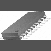
LMX2332LTM National Semiconductor, LMX2332LTM Datasheet - Page 20

LMX2332LTM
Manufacturer Part Number
LMX2332LTM
Description
83F3835
Manufacturer
National Semiconductor
Datasheet
1.LMX2332LTM.pdf
(26 pages)
Specifications of LMX2332LTM
Pll Type
Frequency Synthesis
Frequency
1.1GHz
Supply Current
3mA
Supply Voltage Range
2.7V To 5.5V
Digital Ic Case Style
TSSOP
No. Of Pins
20
Operating Temperature Range
-40°C To +85°C
Rohs Compliant
No
Available stocks
Company
Part Number
Manufacturer
Quantity
Price
Company:
Part Number:
LMX2332LTM
Manufacturer:
NS
Quantity:
8 056
Part Number:
LMX2332LTM
Manufacturer:
NS/国半
Quantity:
20 000
Part Number:
LMX2332LTME
Manufacturer:
NS/国半
Quantity:
20 000
Company:
Part Number:
LMX2332LTMG
Manufacturer:
NS
Quantity:
21
Part Number:
LMX2332LTMG
Manufacturer:
NS/国半
Quantity:
20 000
Company:
Part Number:
LMX2332LTMX
Manufacturer:
NS/TI
Quantity:
3 500
www.national.com
Application Information
A block diagram of the basic phase locked loop is shown in
Figure
LOOP GAIN EQUATIONS
A linear control system model of the phase feedback for a PLL
in the locked state is shown in
is the product of the phase comparator gain (Kφ), the VCO
gain (K
of the feedback counter modulus (N). The passive loop filter
configuration used is displayed in
impedance of the filter is given in
The time constants which determine the pole and zero fre-
quencies of the filter transfer function can be defined as
1.
VCO
/s), and the loop filter gain Z(s) divided by the gain
FIGURE 3. Passive Loop Filter
FIGURE 2. PLL Linear Model
Figure
Figure
Equation
12806 Version 9 Revision 2
FIGURE 1. Basic Charge Pump Phase Locked Loop
1280616
2. The open loop gain
3, while the complex
1.
1280615
(1)
Print Date/Time: 2011/07/11 15:54:42
20
and
The 3rd order PLL Open Loop Gain can be calculated in terms
of frequency, ω, the filter time constants T1 and T2, and the
design constants K
From Equations 2, 3 we can see that the phase term will be
dependent on the single pole and zero such that the phase
margin is determined in
A plot of the magnitude and phase of G(s)H(s) for a stable
loop, is shown in
φ
the gain drops below zero (the cutoff frequency wp of the
loop). In a critically damped system, the amount of phase
margin would be approximately 45 degrees.
If we were now to redefine the cut off frequency, wp', as dou-
ble the frequency which gave us our original loop bandwidth,
wp, the loop response time would be approximately halved.
Because the filter attenuation at the comparison frequency
also diminishes, the spurs would have increased by approxi-
mately 6 dB. In the proposed Fastlock scheme, the higher
spur levels and wider loop filter conditions would exist only
during the initial lock-on phase—just long enough to reap the
benefits of locking faster. The objective would be to open up
the loop bandwidth but not introduce any additional compli-
cations or compromises related to our original design criteria.
We would ideally like to momentarily shift the curve of
4
line, without affecting the relative open loop gain and phase
p
over to a different cutoff frequency, illustrated by the dotted
shows the amount of phase margin that exists at the point
φ(ω) = tan
−1
Figure 4
(ω • T2) − tan
φ
, K
T2 = R2 • C2
VCO
Equation
, and N.
with a solid trace. The parameter
−1
5.
(ω • T1) + 180°
Figure
1280614
(2)
(3)
(4)
(5)


