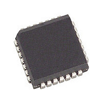
CY7B9234-270JC Cypress Semiconductor Corp, CY7B9234-270JC Datasheet - Page 2

CY7B9234-270JC
Manufacturer Part Number
CY7B9234-270JC
Description
Manufacturer
Cypress Semiconductor Corp
Datasheet
1.CY7B9234-270JC.pdf
(32 pages)
Specifications of CY7B9234-270JC
Lead Free Status / Rohs Status
Not Compliant
Available stocks
Company
Part Number
Manufacturer
Quantity
Price
Company:
Part Number:
CY7B9234-270JC
Manufacturer:
CY
Quantity:
594
Part Number:
CY7B9234-270JC
Manufacturer:
CYPRESS/赛普拉斯
Quantity:
20 000
Document #: 38-02014 Rev. *A
CY7B9234 Transmitter Pin Configuration
Pin Description
CY7B9234 SMPTE HOTLink Transmitter
D
(D
SC/D (D
SVS
(D
ENA
Name
0−7
b − h
j
)
)
HOST
a
)
SVS(D
BISTEN
(D
MODE
TTL In
TTL In
TTL In
TTL In
V
h
I/O
GND
CCQ
)D
RP
j
7
)
5
6
7
8
9
10
11
1213
4 3
Parallel Data Input. Data is clocked into the Transmitter on the rising edge of CKW if ENA is LOW
(or on the next rising CKW with ENN LOW). If ENA and ENN are HIGH, a Null character (K28.5) is
sent. When MODE is HIGH, D
Special Character/Data Select. A HIGH on SC/D when CKW rises causes the transmitter to encode
the pattern on D
using the 8B/10B data alphabet. When MODE is HIGH, SC/D (D
same timing as D
Send Violation Symbol. If SVS is HIGH when CKW rises, a Violation symbol is encoded and sent
while the data on the parallel inputs is ignored. If SVS is LOW, the state of D
the code sent. In normal or test mode, this pin overrides the BIST generator and forces the trans-
mission of a Violation code. When MODE is HIGH (placing the transmitter in unencoded mode), SVS
(D
Enable Parallel Data. If ENA is LOW on the rising edge of CKW, the data is loaded, encoded, and
sent. If ENA and ENN are HIGH, the data inputs are ignored and the Transmitter will insert a Null
character (K28.5) to fill the space between user data. ENA may be held HIGH/LOW continuously or
it may be pulsed with each data byte to be sent. If ENA is being used for data control, ENN will normally
be strapped HIGH, but can be used for BIST function control.
Top View
Description
14
2
PLCC
7B9234
j
) acts as the D
15
1
16
28
1718
2726
Figure 1. SMPTE HOTLink System Connections
25
24
23
22
21
20
19
0−7
FOTO
ENN
ENA
V
CKW
GND
SC/D(D
j
0−7
CCQ
input. SVS has the same timing as D
as a control code (Special Character), while a LOW causes the data to be coded
.
a
)
SERIAL LINK
0, 1, ...7
become D
CY7B9334 Receiver Pin Configuration
b, c,...h
RVS (Q
(Q
V
h
GND
GND
RDY
) Q
CCN
RF
respectively.
0−7
j
7
)
.
5
6
7
8
9
10
11
1213
4 3
Top View
a
14
) acts as D
2
PLCC
7B9334
15
1
28
16
2726
1718
0−7
25
24
23
22
21
20
19
a
and SC/D determines
input. SC/D has the
REFCLK
V
SO
CKR
V
GND
SC/D (Q
CY7B9234
CY7B9334
CCQ
CCQ
HOST
Page 2 of 32
a
)
[+] Feedback


