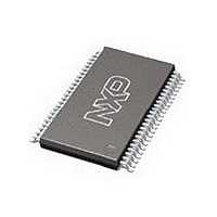
CBT16210DGG NXP Semiconductors, CBT16210DGG Datasheet - Page 5

CBT16210DGG
Manufacturer Part Number
CBT16210DGG
Description
Manufacturer
NXP Semiconductors
Datasheet
1.CBT16210DGG.pdf
(8 pages)
Specifications of CBT16210DGG
Logic Family
CBT
Number Of Bits
20
Number Of Elements
2
Technology
CMOS
Low Level Output Current
128mA
On Resistance
10Ohm
Propagation Delay Time
6.5ns
Package Type
TSSOP
Operating Temp Range
-40C to 85C
Operating Temperature Classification
Industrial
Operating Supply Voltage (min)
4.5V
Operating Supply Voltage (typ)
5V
Operating Supply Voltage (max)
5.5V
Quiescent Current
20uA
Pin Count
48
Mounting
Surface Mount
Lead Free Status / Rohs Status
Compliant
1. This parameter is warranted but not production tested. The propagation delay is based on the RC time constant of the typical on-state
Philips Semiconductors
AC CHARACTERISTICS
GND = 0 V; t
NOTES:
AC WAVEFORMS
V
2000 Oct 12
M
Output Control
20-bit bus switch with 10-bit output enables
OUTPUT
Waveform 1. Input (An) to Output (Yn) Propagation Delays
resistance of the switch and a load capacitance of 50 pF, when driven by an ideal voltage source (zero output impedance).
Waveform 1
Waveform 2
= 1.5 V, V
SYMBOL
INPUT
S1 at Open
(see Note)
(see Note)
(Low-level
Waveform 2. 3-State Output Enable and Disable Times
S1 at 7 V
enabling
t
t
t
t
PZH
PHZ
t
PZL
PLZ
Output
Output
pd
Note:
Waveform 1 is for an output with internal conditions such that
the output is low except when disabled by the output control.
Waveform 2 is for an output with internal conditions such that
the output is high except when disabled by the output control.
t
R;
PZH
IN
t
PZL
C
= GND to 3.0 V
L
1.5V
= 50 pF
Propagation delay
Output enable time to HIGH level
Output disable time from HIGH level
Output enable time to LOW level
Output disable time from LOW level
t
PLH
1.5 V
1.5 V
1.5 V
1.5V
t
PHZ
1
t
PARAMETER DESCRIPTION
PLZ
1.5V
1.5 V
t
PHL
V
V
OL
OH
+ 0.3V
– 0.3V
1.5V
SA00029
SA00028
3V
0V
3.5V
V
V
0V
OL
OH
3 V
0 V
V
V
OH
OL
5
TEST CIRCUIT AND WAVEFORMS
DEFINITIONS
C
From Output
Under Test
L
=
–40 C to +85 C V
C
Load capacitance includes jig and probe capacitance;
see AC CHARACTERISTICS for value.
L
Min
1.5
1.0
1.5
1.5
= 50 pF
t
t
PHZ
PLZ
TEST
LIMITS
Mean
t
pd
/t
/t
3.3
2.4
4.0
3.8
PZL
PZH
500
CC
Load Circuit
500
= 5 V
open
open
7 V
S1
Max
250
5.0
4.5
6.5
6.0
0.5 V
S1
CBT16210
Product specification
7 V
GND
SA00012
Open
UNITS
ps
ns
ns
ns
ns


