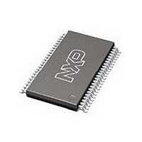
CBT16210DGG NXP Semiconductors, CBT16210DGG Datasheet - Page 4

CBT16210DGG
Manufacturer Part Number
CBT16210DGG
Description
Manufacturer
NXP Semiconductors
Datasheet
1.CBT16210DGG.pdf
(8 pages)
Specifications of CBT16210DGG
Logic Family
CBT
Number Of Bits
20
Number Of Elements
2
Technology
CMOS
Low Level Output Current
128mA
On Resistance
10Ohm
Propagation Delay Time
6.5ns
Package Type
TSSOP
Operating Temp Range
-40C to 85C
Operating Temperature Classification
Industrial
Operating Supply Voltage (min)
4.5V
Operating Supply Voltage (typ)
5V
Operating Supply Voltage (max)
5.5V
Quiescent Current
20uA
Pin Count
48
Mounting
Surface Mount
Lead Free Status / Rohs Status
Compliant
1. Stresses beyond those listed may cause permanent damage to the device. These are stress ratings only and functional operation of the
2. The performance capability of a high-performance integrated circuit in conjunction with its thermal environment can create junction
3. The input and output voltage ratings may be exceeded if the input and output current ratings are observed.
1. All typical values are at V
2. This is the increase in supply current for each input that is at the specified TTL voltage level rather than V
3. Measured by the voltage drop between the A and the B terminals at the indicated current through the switch.
Philips Semiconductors
ABSOLUTE MAXIMUM RATINGS
NOTES:
RECOMMENDED OPERATING CONDITIONS
DC ELECTRICAL CHARACTERISTICS
NOTES:
2000 Oct 12
SYMBOL
SYMBOL
SYMBOL
SYMBOL
C
20-bit bus switch with 10-bit output enables
device at these or any other conditions beyond those indicated under “recommended operating conditions” is not implied. Exposure to
absolute-maximum-rated conditions for extended periods may affect device reliability.
temperatures which are detrimental to reliability. The maximum junction temperature of this integrated circuit should not exceed 150 C.
On-state resistance is determined by the lowest voltage of the two (A or B) terminals.
V
IO(OFF)
T
I
V
V
T
r
OUT
V
V
I
V
amb
V
I
OUT
CC
C
on
V
I
stg
CC
IK
CC
I
I
CC
IH
IK
IL
I
P
I
I
3
3
DC supply voltage
DC input diode current
DC input voltage
DC output voltage
DC output current
Storage temperature range
DC supply voltage
High-level input voltage
Low-level Input voltage
Operating free-air temperature range
Input clamp voltage
Output high pass voltage
Input leakage current
Input leakage current
Quiescent supply current
Additional supply current per
input pin
Control pins
Port capacitance in off state
PARAMETER
2
CC
PARAMETER
3
= 5 V, T
3
amb
2
1, 2
= 25 C
PARAMETER
PARAMETER
V
V
V
V
V
1OE=2OE=GND
V
other inputs at V
V
V
V
V
V
CC
in
CC
CC
CC
CC
I
O
CC
CC
CC
= 3 V or 0
– V
= 3 V or 0, OE = V
= 4.5 V; I
= 0 V; V
= 5.5 V; V
= 5.5 V; I
= 5.5 V, one input at 3.4 V,
= 4.5 V; V
= 4.5 V; V
= 4.5 V; V
cc
= 5.0 V, I
I
I
= 5.5 V
O
TEST CONDITIONS
I
1
1
1
= –18 mA
= GND or 5.5 V
= 0, V
CC
= 0 V; I
= 0 V; I
= 2.4 V; I
OUT
or GND
output in Off or High state
I
CC
= –100 A
= V
4
I
I
output in Low state
= 64 mA
= 30 mA
I
CONDITIONS
CC
= –15 mA
or GND;
V
I
< 0
Min
–40
4.5
2.0
Min
3.4
T
amb
LIMITS
CC
–0.5 to +7.0
–0.5 to +7.0
–0.5 to +5.5
= –40 C to +85 C
–65 to 150
or GND
RATING
LIMITS
Typ
–50
128
3.6
4.5
6.9
10
5
5
1
Max
+85
5.5
0.8
CBT16210
Product specification
Max
–1.2
3.9
2.5
10
20
15
7
7
1
UNIT
UNIT
UNIT
mA
mA
V
V
V
V
V
V
UNIT
C
C
mA
pF
pF
V
V
A
A
A


