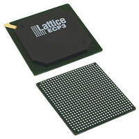
LFE3-35EA-8FN672I Lattice, LFE3-35EA-8FN672I Datasheet - Page 29

LFE3-35EA-8FN672I
Manufacturer Part Number
LFE3-35EA-8FN672I
Description
IC FPGA 33.3K LUTS 310I/O FN672
Manufacturer
Lattice
Series
ECP3r
Datasheets
1.LFE3-150EA-7FN672C.pdf
(136 pages)
2.LFE3-35EA-8FN672I.pdf
(4 pages)
3.LFE3-35EA-8FN672I.pdf
(21 pages)
Specifications of LFE3-35EA-8FN672I
Number Of Logic Elements/cells
33000
Number Of Labs/clbs
4125
Total Ram Bits
1358848
Number Of I /o
310
Number Of Gates
-
Voltage - Supply
1.14 V ~ 1.26 V
Mounting Type
Surface Mount
Operating Temperature
-40°C ~ 100°C
Package / Case
672-BBGA
Lead Free Status / Rohs Status
Lead free / RoHS Compliant
Other names
220-1163
- LFE3-150EA-7FN672C PDF datasheet
- LFE3-35EA-8FN672I PDF datasheet #2
- LFE3-35EA-8FN672I PDF datasheet #3
- Current page: 29 of 136
- Download datasheet (3Mb)
Lattice Semiconductor
MMAC DSP Element
The LatticeECP3 supports a MAC with two multipliers. This is called Multiply Multiply Accumulate or MMAC. In this
case, the two operands, AA and AB, are multiplied and the result is added with the previous accumulated value and
with the result of the multiplier operation of operands BA and BB. This accumulated value is available at the output.
The user can enable the input and pipeline registers, but the output register is always enabled. The output register
is used to store the accumulated value. The ALU is configured as the accumulator in the sysDSP slice. A registered
overflow signal is also available. The overflow conditions are provided later in this document. Figure 2-28 shows the
MMAC sysDSP element.
Figure 2-28. MMAC sysDSP Element
DSP Slice
Previous
IR = Input Register
PR = Pipeline Register
OR = Output Register
FR = Flag Register
Rounding
SRIB
SRIA
C_ALU
A_ALU
CIN
0
IR
C
IR
AA
MULTA
OR
PR
AMUX
A_ALU
IR
From FPGA Core
AB
To FPGA Core
0
R = Logic (B, C)
R= A ± B ± C
2-26
OR
PR
IR
OPCODE
FR
0
=
=
B_ALU
BMUX
IR
ALU
BA
MULTB
LatticeECP3 Family Data Sheet
OR
PR
IR
BB
IR
COUT
SROB
SROA
DSP Slice
Next
Architecture
Related parts for LFE3-35EA-8FN672I
Image
Part Number
Description
Manufacturer
Datasheet
Request
R
Part Number:
Description:
33.3K LUTS, 295 I/O, 1.2V, -6 SPEED, PB-FREE
Manufacturer:
LATTICE SEMICONDUCTOR
Datasheet:
Part Number:
Description:
FPGA LatticeECP3™ Family 33000 Cells 65nm Technology 1.2V 484-Pin FBGA
Manufacturer:
LATTICE SEMICONDUCTOR
Datasheet:

Part Number:
Description:
IC FPGA 33.3KLUTS 133I/O 256BGA
Manufacturer:
Lattice
Datasheet:

Part Number:
Description:
IC FPGA 33.3KLUTS 133I/O 256BGA
Manufacturer:
Lattice
Datasheet:

Part Number:
Description:
IC FPGA 33.3KLUTS 295I/O 484BGA
Manufacturer:
Lattice
Datasheet:

Part Number:
Description:
IC FPGA 33.3KLUTS 310I/O 672BGA
Manufacturer:
Lattice
Datasheet:

Part Number:
Description:
IC FPGA 33.3KLUTS 310I/O 672BGA
Manufacturer:
Lattice
Datasheet:

Part Number:
Description:
IC FPGA 35KLUTS 133I/O 256-BGA
Manufacturer:
Lattice
Datasheet:

Part Number:
Description:
IC FPGA 35KLUTS 133I/O 256-BGA
Manufacturer:
Lattice
Datasheet:

Part Number:
Description:
IC FPGA 33KLUTS 295I/O 484-BGA
Manufacturer:
Lattice
Datasheet:

Part Number:
Description:
IC FPGA 33KLUTS 295I/O 484-BGA
Manufacturer:
Lattice
Datasheet:

Part Number:
Description:
IC FPGA 35KLUTS 133I/O 256-BGA
Manufacturer:
Lattice
Datasheet:

Part Number:
Description:
IC FPGA 33KLUTS 295I/O 484-BGA
Manufacturer:
Lattice
Datasheet:

Part Number:
Description:
IC FPGA 33.3KLUTS 672FPBGA
Manufacturer:
Lattice
Datasheet:

Part Number:
Description:
IC FPGA 33.3KLUTS 256FTBGA
Manufacturer:
Lattice
Datasheet:


