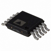
ADG787BRMZ Analog Devices Inc, ADG787BRMZ Datasheet - Page 3

ADG787BRMZ
Manufacturer Part Number
ADG787BRMZ
Description
IC MUX/DEMUX DUAL 2X1 10MSOP
Manufacturer
Analog Devices Inc
Type
Analog Switchr
Datasheet
1.ADG787BRMZ.pdf
(16 pages)
Specifications of ADG787BRMZ
Function
Multiplexer/Demultiplexer
Circuit
2 x 2:1
On-state Resistance
3 Ohm
Voltage Supply Source
Single Supply
Voltage - Supply, Single/dual (±)
1.8 V ~ 5.5 V
Current - Supply
0.005µA
Operating Temperature
-40°C ~ 85°C
Mounting Type
Surface Mount
Package / Case
10-TFSOP, 10-MSOP (0.118", 3.00mm Width)
Analog Switch Type
SPDT
No. Of Channels
2
Bandwidth
145MHz
On State Resistance Max
3.45ohm
Turn Off Time
3ns
Turn On Time
13ns
Supply Voltage Range
1.8V To 5.5V
Multiplexer Configuration
Dual SPDT
Number Of Inputs
2
Number Of Outputs
4
Number Of Channels
2
Analog Switch On Resistance
5.75@3.6VOhm
Analog Switch Turn On Time
30ns
Analog Switch Turn Off Time
6ns
Package Type
MSOP
Power Supply Requirement
Single
Single Supply Voltage (min)
1.8V
Single Supply Voltage (typ)
3/5V
Single Supply Voltage (max)
5.5V
Dual Supply Voltage (min)
Not RequiredV
Dual Supply Voltage (typ)
Not RequiredV
Dual Supply Voltage (max)
Not RequiredV
Power Dissipation
0.0001W
Supply Current
0.001mA
Mounting
Surface Mount
Pin Count
10
Operating Temp Range
-40C to 85C
Operating Temperature Classification
Industrial
Lead Free Status / RoHS Status
Lead free / RoHS Compliant
Lead Free Status / RoHS Status
Lead free / RoHS Compliant, Lead free / RoHS Compliant
Available stocks
Company
Part Number
Manufacturer
Quantity
Price
Company:
Part Number:
ADG787BRMZ
Manufacturer:
TI
Quantity:
104
Part Number:
ADG787BRMZ-REEL7
Manufacturer:
ADI/亚德诺
Quantity:
20 000
SPECIFICATIONS
V
Table 1.
Parameter
ANALOG SWITCH
LEAKAGE CURRENTS
DIGITAL INPUTS
DYNAMIC CHARACTERISTICS
POWER REQUIREMENTS
1
2
Temperature ranges: B version: −40°C to +85°C for the MSOP and LFCSP packages, and −25°C to +85°C for the WLCSP package.
Guaranteed by design, not production tested.
DD
Analog Signal Range
On Resistance (R
On Resistance Match Between Channels (ΔR
On Resistance Flatness (R
Source Off Leakage, I
Channel On Leakage, I
Input High Voltage, V
Input Low Voltage, V
Input Current
C
t
t
Propagation Delay Skew, t
Break-Before-Make Time Delay (t
Charge Injection
Off Isolation
Channel-to-Channel Crosstalk
Total Harmonic Distortion (THD + N)
Insertion Loss
−3 dB Bandwidth
C
C
I
DD
ON
OFF
IN
S
D
= 4.2 V to 5.5 V, GND = 0 V, unless otherwise noted.
I
, C
(OFF)
, Digital Input Capacitance
INL
S
or I
(ON)
INH
ON
)
INL
S
INH
(OFF)
D
, I
S
FLAT (ON)
(ON)
SKEW
2
)
BBM
)
ON
)
+25°C
2.5
3
0.02
0.65
0.8
±0.05
±0.05
0.005
2.5
13
19
3
5
0.06
10
14
−63
−110
−63
0.03
−0.2
145
16
40
0.005
Rev. A | Page 3 of 16
B Version
0 to V
3.45
0.1
0.95
2.0
0.8
±0.1
22
6
0.15
5
1
DD
1
Unit
V
Ω typ
Ω max
Ω typ
Ω max
Ω typ
Ω max
nA typ
nA typ
V min
V max
μA typ
μA max
pF typ
ns typ
ns max
ns typ
ns max
ns typ
ns max
ns typ
ns min
pC typ
dB typ
dB typ
dB typ
%
dB typ
MHz typ
pF typ
pF typ
μA typ
μA max
Test Conditions/Comments
V
See Figure 28
V
V
I
V
V
V
V
R
V
R
V
C
R
V
V
R
S1A to S2A/S1B to S2B; R
f = 1 MHz; see Figure 37
S1A to S1B/S2A to S2B; R
f = 1 MHz; see Figure 36
R
R
R
V
Digital inputs = 0 V or 5.5 V
S
L
L
L
L
L
L
L
DD
DD
DD
DD
S
S
IN
S
S
L
S1
D
DD
= 10 mA
= 50 Ω, C
= 50 Ω, C
= 50 Ω, C
= 50 Ω, C
= 32 Ω, f = 20 Hz to 20 kHz, V
= 50 Ω, C
= 50 Ω, C
= 1 V/4.5 V, V
= V
= 3 V; see Figure 31
= 3 V; see Figure 31
= 50 pF; V
= 1 V, R
= V
= V
= 4.2 V, V
= 4.2 V, V
= 4.2 V, V
= 5.5 V
= 5.5 V
D
INL
S2
= 1 V or 4.5 V; see Figure 30
= 3 V; see Figure 32
or V
S
= 0 Ω, C
L
L
L
L
L
L
S
S
S
S
INH
= 35 pF
= 35 pF
= 35 pF
= 5 pF, f = 1 MHz; see Figure 34
= 5 pF; see Figure 36
= 5 pF; see Figure 36
= 3 V
= 0 V to V
= 3.5 V, I
= 0 V to V
D
= 4.5 V/1 V; see Figure 29
L
= 1 nF; see Figure 33
S
DD
= 10 mA
DD
L
L
, I
= 50 Ω, C
= 50 Ω, C
S
= 10 mA
S
= 2 V p-p
ADG787
L
L
= 5 pF,
= 5 pF,


