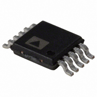
ADG787BRMZ Analog Devices Inc, ADG787BRMZ Datasheet - Page 13

ADG787BRMZ
Manufacturer Part Number
ADG787BRMZ
Description
IC MUX/DEMUX DUAL 2X1 10MSOP
Manufacturer
Analog Devices Inc
Type
Analog Switchr
Datasheet
1.ADG787BRMZ.pdf
(16 pages)
Specifications of ADG787BRMZ
Function
Multiplexer/Demultiplexer
Circuit
2 x 2:1
On-state Resistance
3 Ohm
Voltage Supply Source
Single Supply
Voltage - Supply, Single/dual (±)
1.8 V ~ 5.5 V
Current - Supply
0.005µA
Operating Temperature
-40°C ~ 85°C
Mounting Type
Surface Mount
Package / Case
10-TFSOP, 10-MSOP (0.118", 3.00mm Width)
Analog Switch Type
SPDT
No. Of Channels
2
Bandwidth
145MHz
On State Resistance Max
3.45ohm
Turn Off Time
3ns
Turn On Time
13ns
Supply Voltage Range
1.8V To 5.5V
Multiplexer Configuration
Dual SPDT
Number Of Inputs
2
Number Of Outputs
4
Number Of Channels
2
Analog Switch On Resistance
5.75@3.6VOhm
Analog Switch Turn On Time
30ns
Analog Switch Turn Off Time
6ns
Package Type
MSOP
Power Supply Requirement
Single
Single Supply Voltage (min)
1.8V
Single Supply Voltage (typ)
3/5V
Single Supply Voltage (max)
5.5V
Dual Supply Voltage (min)
Not RequiredV
Dual Supply Voltage (typ)
Not RequiredV
Dual Supply Voltage (max)
Not RequiredV
Power Dissipation
0.0001W
Supply Current
0.001mA
Mounting
Surface Mount
Pin Count
10
Operating Temp Range
-40C to 85C
Operating Temperature Classification
Industrial
Lead Free Status / RoHS Status
Lead free / RoHS Compliant
Lead Free Status / RoHS Status
Lead free / RoHS Compliant, Lead free / RoHS Compliant
Available stocks
Company
Part Number
Manufacturer
Quantity
Price
Company:
Part Number:
ADG787BRMZ
Manufacturer:
TI
Quantity:
104
Part Number:
ADG787BRMZ-REEL7
Manufacturer:
ADI/亚德诺
Quantity:
20 000
TERMINOLOGY
I
Positive supply current.
V
Analog voltage on Terminal D and Terminal S.
R
Ohmic resistance between D and S.
R
Flatness is defined as the difference between the maximum and
minimum value of on resistance as measured.
ΔR
On resistance match between any two channels.
I
Source leakage current with the switch off.
I
Drain leakage current with the switch off.
I
Channel leakage current with the switch on.
V
Maximum input voltage for Logic 0.
V
Minimum input voltage for Logic 1.
I
Input current of the digital input.
C
Off switch source capacitance. Measured with reference to
ground.
C
Off switch drain capacitance. Measured with reference to
ground.
C
On switch capacitance. Measured with reference to ground.
C
Digital input capacitance.
t
Delay time between the 50% and the 90% points of the digital
input and switch on condition.
ON
DD
S
D
D
INL
ON
FLAT (ON)
S
D
D
IN
D
INL
INH
, I
(OFF)
(OFF)
, C
(OFF)
(V
ON
(OFF)
(I
S
(ON)
INH
S
S
)
(ON)
)
Rev. A | Page 13 of 16
t
Delay time between the 50% and the 90% points of the digital
input and switch off condition.
t
On or off time measured between the 80% points of both
switches when switching from one to another.
Charge Injection
A measure of the glitch impulse transferred from the digital
input to the analog output during on-off switching.
Off Isolation
A measure of unwanted signal coupling through an off switch.
Crosstalk
A measure of unwanted signal that is coupled from one channel
to another as a result of parasitic capacitance.
−3 dB Bandwidth
The frequency at which the output is attenuated by 3 dB.
On Response
The frequency response of the on switch.
Insertion Loss
The loss due to the on resistance of the switch.
THD + N
The ratio of the harmonic amplitudes plus noise of a signal, to
the fundamental.
T
The measure of the variation in propagation delay between each
channel.
Rise Time Delay
The rise time of a signal is a measure of the time for the signal
to rise from 10% of the ON level to 90% of the ON level. Rise
time delay is the difference between the rise time, measured at
the input, and the rise time, measured at the output.
Fall Time Delay
The fall time of a signal is a measure of the time for the signal to
fall from 90% of the ON level to 10% of the ON level. Fall time
delay is the difference between the fall time, measured at the
input, and the fall time, measured at the output.
Rise-Time-to-Fall-Time Mismatch
This is the absolute value between the variation in the fall time
and the rise time, measured at the output.
OFF
BBM
SKEW
ADG787


