MAX4906FELB+T Maxim Integrated Products, MAX4906FELB+T Datasheet - Page 12
MAX4906FELB+T
Manufacturer Part Number
MAX4906FELB+T
Description
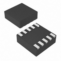
IC USB SWITCH DUAL 1X2 10UDFN
Manufacturer
Maxim Integrated Products
Datasheet
1.MAX4906FELBT.pdf
(14 pages)
Specifications of MAX4906FELB+T
Function
USB Switch
Circuit
2 x SPDT
On-state Resistance
7 Ohm
Voltage Supply Source
Single Supply
Voltage - Supply, Single/dual (±)
3 V ~ 3.6 V
Current - Supply
120µA
Operating Temperature
-40°C ~ 85°C
Mounting Type
Surface Mount
Package / Case
10-µDFN
Supply Voltage (max)
3.6 V
Supply Voltage (min)
3 V
Maximum Operating Temperature
+ 85 C
Minimum Operating Temperature
- 40 C
Mounting Style
SMD/SMT
Number Of Switches
Dual
Switch Configuration
SPDT
Lead Free Status / RoHS Status
Lead free / RoHS Compliant
Other names
MAX4906FELB+T
MAX4906FELB+TTR
MAX4906FELB+TTR


High-/Full-Speed USB 2.0 Switches
ideal for routing USB data lines (see Figure 7) and for
applications that require switching between multiple
USB hosts (see Figure 8). The MAX4907/MAX4907F
can be used in applications that require different data
types to share the same pins (see Figure 9); however,
the shared device must be capable of going into the tri-
state mode. The MAX4906F/MAX4907F also feature
+5.5V fault protection to guard systems against shorts
to the USB bus voltage. The fault-protected versions
are recommended for all USB applications.
Figure 7. MAX4906/MAX4906F USB Data Routing
Figure 8. MAX4906/MAX4906F Switching Between Multiple
USB Hosts
12
______________________________________________________________________________________
TRANSCEIVER
TRANSCEIVER
ASIC II
ASIC I
TRANSCEIVER
USB
USB
USB
D+
D+
D-
D-
COM1
COM2
MAX4906F
NC1
NO1
NC2
NO2
MAX4906/
MAX4906F
MAX4906/
NC1
NO1
NC2
NO2
COM1
COM2
USB
USB
USB
USB
V
GND
BUS
D+
0
1
0
1
D-
+
+
-
-
CONNECTOR
USB
The wide bandwidth of the MAX4906/MAX4906F/
MAX4907/MAX4907F meets the needs of 10/100 Ethernet
switching. These devices switch the signals from two
interface transformers and connect the signals to a single
10/100 Base-T Ethernet PHY, simplifying docking station
design and reducing manufacturing costs.
Caution: Do not exceed the absolute maximum rat-
ings because stresses beyond the listed ratings
may cause permanent damage to the device.
Proper power-supply sequencing is recommended for
all CMOS devices. Always apply V+ before applying
analog signals, especially if the analog signal is not
current limited.
High-speed switches require proper layout and design
procedures for optimum performance. Keep design-
controlled-impedance PC board traces as short as pos-
sible. Ensure that bypass capacitors are as close to the
device as possible. Use large ground planes where
possible.
Figure 9. MAX4907/MAX4907F USB/SPI/GPIO Switch
SPI/GPIO
DEVICE
CLOCK
DATA
EN
DATA PINS
SHARED
TRI-STATE
ENABLE
Power-Supply Sequencing
NO1
NO2
MAX4907F
MAX4907/
Ethernet Switching
COM1
COM2
TRANSCEIVER
Layout
USB
Related parts for MAX4906FELB+T
Image
Part Number
Description
Manufacturer
Datasheet
Request
R

Part Number:
Description:
MAX7528KCWPMaxim Integrated Products [CMOS Dual 8-Bit Buffered Multiplying DACs]
Manufacturer:
Maxim Integrated Products
Datasheet:
Part Number:
Description:
Single +5V, fully integrated, 1.25Gbps laser diode driver.
Manufacturer:
Maxim Integrated Products
Datasheet:
Part Number:
Description:
Single +5V, fully integrated, 155Mbps laser diode driver.
Manufacturer:
Maxim Integrated Products
Datasheet:
Part Number:
Description:
VRD11/VRD10, K8 Rev F 2/3/4-Phase PWM Controllers with Integrated Dual MOSFET Drivers
Manufacturer:
Maxim Integrated Products
Datasheet:
Part Number:
Description:
Highly Integrated Level 2 SMBus Battery Chargers
Manufacturer:
Maxim Integrated Products
Datasheet:
Part Number:
Description:
Current Monitor and Accumulator with Integrated Sense Resistor; ; Temperature Range: -40°C to +85°C
Manufacturer:
Maxim Integrated Products
Part Number:
Description:
TSSOP 14/A�/RS-485 Transceivers with Integrated 100O/120O Termination Resis
Manufacturer:
Maxim Integrated Products
Part Number:
Description:
TSSOP 14/A�/RS-485 Transceivers with Integrated 100O/120O Termination Resis
Manufacturer:
Maxim Integrated Products
Part Number:
Description:
QFN 16/A�/AC-DC and DC-DC Peak-Current-Mode Converters with Integrated Step
Manufacturer:
Maxim Integrated Products
Part Number:
Description:
TDFN/A/65V, 1A, 600KHZ, SYNCHRONOUS STEP-DOWN REGULATOR WITH INTEGRATED SWI
Manufacturer:
Maxim Integrated Products
Part Number:
Description:
Integrated Temperature Controller f
Manufacturer:
Maxim Integrated Products
Part Number:
Description:
SOT23-6/I�/45MHz to 650MHz, Integrated IF VCOs with Differential Output
Manufacturer:
Maxim Integrated Products
Part Number:
Description:
SOT23-6/I�/45MHz to 650MHz, Integrated IF VCOs with Differential Output
Manufacturer:
Maxim Integrated Products
Part Number:
Description:
EVALUATION KIT/2.4GHZ TO 2.5GHZ 802.11G/B RF TRANSCEIVER WITH INTEGRATED PA
Manufacturer:
Maxim Integrated Products
Part Number:
Description:
QFN/E/DUAL PCIE/SATA HIGH SPEED SWITCH WITH INTEGRATED BIAS RESISTOR
Manufacturer:
Maxim Integrated Products
Datasheet: