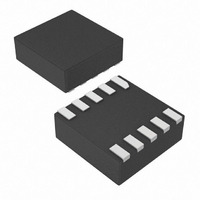
MAX4906FELB+T Maxim Integrated Products, MAX4906FELB+T Datasheet - Page 11

MAX4906FELB+T
Manufacturer Part Number
MAX4906FELB+T
Description
IC USB SWITCH DUAL 1X2 10UDFN
Manufacturer
Maxim Integrated Products
Datasheet
1.MAX4906FELBT.pdf
(14 pages)
Specifications of MAX4906FELB+T
Function
USB Switch
Circuit
2 x SPDT
On-state Resistance
7 Ohm
Voltage Supply Source
Single Supply
Voltage - Supply, Single/dual (±)
3 V ~ 3.6 V
Current - Supply
120µA
Operating Temperature
-40°C ~ 85°C
Mounting Type
Surface Mount
Package / Case
10-µDFN
Supply Voltage (max)
3.6 V
Supply Voltage (min)
3 V
Maximum Operating Temperature
+ 85 C
Minimum Operating Temperature
- 40 C
Mounting Style
SMD/SMT
Number Of Switches
Dual
Switch Configuration
SPDT
Lead Free Status / RoHS Status
Lead free / RoHS Compliant
Other names
MAX4906FELB+T
MAX4906FELB+TTR
MAX4906FELB+TTR
The MAX4906/MAX4906F/MAX4907/MAX4907F provide
a single-digit control logic input, IN. IN controls the
position of the switches as shown in the Functional
Diagram/Truth Table. Driving IN rail-to-rail minimizes
power consumption. With a +3.0V to +3.6V supply volt-
age range, these devices are +1.4V logic compatible.
The on-resistance of the MAX4906/MAX4906F/
MAX4907/MAX4907F is very low and stable as the ana-
log input signals are swept from ground to V+ (see the
Typical Operating Characteristics). These switches are
bidirectional, allowing NO_, NC_, and COM_ to be con-
figured as either inputs or outputs.
The MAX4906F and MAX4907F feature +5.5V fault pro-
tection to COM1 and COM2. Fault protection prevents
these switches from being damaged due to shorts to
the USB bus voltage rail.
NO1
NC1
NO2
NC2
IN
Overvoltage Fault Protection
______________________________________________________________________________________
SHDN/EN
V+
0
0
1
MAX4906/MAX4906F
Analog Signal Levels
IN
0
1
x
Digital Control Input
MAX4906/MAX4906F
GND
High-/Full-Speed USB 2.0 Switches
NO1
NO2
OFF
OFF
ON
SHDN/EN
NC1
NC2
OFF
OFF
ON
COM1
COM2
The MAX4906/MAX4906F feature a shutdown mode
that reduces the quiescent current supply to less than
2µA. Drive SHDN/EN high to place the devices in high-
impedance mode. When SHDN/EN is driven low, the
devices are normal in operation.
The MAX4907/MAX4907F feature a SHDN input that
reduces the quiescent current supply to less than 2µA.
Drive SHDN high to place the devices in low current
mode. The devices can be used in low current mode, but
with a reduced analog voltage range of 0 < V
1.5V and reduced performance. When SHDN is driven
low, the MAX4907/MAX4907F are in normal operation.
The MAX4906/MAX4906F/MAX4907/MAX4907F analog
switches are fully compliant with the USB 2.0 specifica-
tion. The low on-resistance and low on-capacitance of
these switches make them ideal for high-performance
switching applications. The MAX4906/MAX4906F are
Functional Diagram/Truth Table
NO1
NO2
IN
SHDN
0
0
1
1
V+
Applications Information
MAX4907/MAX4907F
IN
0
1
0
1
MAX4907/MAX4907F
GND
COM1- NO1
COM2- NO1
OFF
OFF
ON
ON
SHDN
Shutdown Mode
USB Switching
COM1
COM2
ANALOG
11
<


