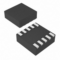
MAX4906FELB+T Maxim Integrated Products, MAX4906FELB+T Datasheet - Page 10

MAX4906FELB+T
Manufacturer Part Number
MAX4906FELB+T
Description
IC USB SWITCH DUAL 1X2 10UDFN
Manufacturer
Maxim Integrated Products
Datasheet
1.MAX4906FELBT.pdf
(14 pages)
Specifications of MAX4906FELB+T
Function
USB Switch
Circuit
2 x SPDT
On-state Resistance
7 Ohm
Voltage Supply Source
Single Supply
Voltage - Supply, Single/dual (±)
3 V ~ 3.6 V
Current - Supply
120µA
Operating Temperature
-40°C ~ 85°C
Mounting Type
Surface Mount
Package / Case
10-µDFN
Supply Voltage (max)
3.6 V
Supply Voltage (min)
3 V
Maximum Operating Temperature
+ 85 C
Minimum Operating Temperature
- 40 C
Mounting Style
SMD/SMT
Number Of Switches
Dual
Switch Configuration
SPDT
Lead Free Status / RoHS Status
Lead free / RoHS Compliant
Other names
MAX4906FELB+T
MAX4906FELB+TTR
MAX4906FELB+TTR
The MAX4906/MAX4906F/MAX4907/MAX4907F analog
switches are targeted for USB 2.0 high-speed
(480Mbps) switching applications. These devices still
meet USB low- and full-speed requirements and are
suitable for 10/100 Ethernet switching. The MAX4906/
MAX4906F feature two SPDT switches, while the
MAX4907/MAX4907F feature two SPST switches. The
MAX4907/MAX4907F switch configurations have a low
7Ω (max) on-resistance and 7pF (max) on-capacitance.
High-/Full-Speed USB 2.0 Switches
Figure 5. MAX4906F/MAX4907F Fault-Protection Response/Recovery Time
Figure 6. Charge Injection
10
______________________________________________________________________________________
MAX4906/MAX4906F
MAX4907/MAX4907F
V
GEN
R
GEN
Detailed Description
OR NO_
NC_
GND
VCOM_
VNO_
VNC_
IN
V
IL
TO V
COM_
V+
V+
2.5V
V
PF
IH
t
PF
Test Circuits/Timing Diagrams (continued)
C
L
2.5V
V
OUT
t
The MAX4906/MAX4906F/MAX4907/MAX4907F are fully
specified to operate from a single +3.0V to +3.6V supply
and are available with +5.5V fault protection (MAX4906F/
MAX4907F). When operating from a +3.0V to +3.6V sup-
ply, the low threshold of these devices permits them to
be used with logic levels as low as 1.4V.The
MAX4906/MAX4906F/MAX4907/MAX4907F are based
on a charge-pump-assisted n-channel architecture and
thus operate at 300µA (max) quiescent current. These
devices all feature a shutdown input to reduce the quies-
cent current to less than 2µA (max).
FPR
V
OUT
IN
1.5V
IN
OFF
OFF
LOGIC INPUT WAVEFORMS INVERTED FOR SWITCHES
THAT HAVE THE OPPOSITE LOGIC SENSE.
Q = (ΔV
5V
3V
0V
3V
0V
ON
ON
OUT
)(C
L
)
ΔV
OUT
OFF
OFF


