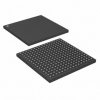
DS33X161+ Maxim Integrated Products, DS33X161+ Datasheet - Page 252

DS33X161+
Manufacturer Part Number
DS33X161+
Description
IC MAPPING ETHERNET 256CSBGA
Manufacturer
Maxim Integrated Products
Datasheet
1.DS33X11.pdf
(375 pages)
Specifications of DS33X161+
Applications
Data Transport
Interface
Parallel/Serial
Voltage - Supply
1.8V, 2.5V, 3.3V
Package / Case
256-CSBGA
Mounting Type
Surface Mount
Lead Free Status / RoHS Status
Lead free / RoHS Compliant
- Current page: 252 of 375
- Download datasheet (3Mb)
501h:
Default
10.7.2 VCAT Receive Register Description
Note: Some registers are on a per-WAN-port basis.
Register Name:
Register Description:
Register Address:
500h:
Default
Bit 12: Receive VCAT and Data Path Enable for VCG 4 (RVEN4) Data path reset and enable. This bit function is
not available in device revision A1 (GL.IDR.REVn=000).
Bit 11: Receive GID Bit Convention (RGIDBC) Controls all 4 VCGs. This bit is only used when TGIDM = 1
Bit 10: Receive VCAT and Data Path Enable for VCG 3 (RVEN3) Data path Reset disable. This bit function is not
available in device revision A1 (GL.IDR.REVn=000).
Bit 9: Receive VCAT and Data Path Enable for VCG 2 (RVEN2) Data path Reset disable. This bit function is not
available in device revision A1 (GL.IDR.REVn=000).
Bit 8: Receive VCAT and Data Path Enable for VCG 1 (RVEN1) Data path Reset disable. This bit function is not
available in device revision A1 (GL.IDR.REVn=000).
Bit 5: Sequence Value Integration Disable (SVINTD) Integration of sequence values applies to non-LCAS
operation only.
Bit 4: T3/E3 or T1/E1 Selection for WAN Group 4 (T3T1WG4)
Bit 3: T3/E3 or T1/E1 Selection for WAN Group 3 (T3T1WG3)
Rev: 063008
________________________________________________ DS33X162/X161/X82/X81/X42/X41/X11/W41/W11
0 = VCAT Block is disabled and held in reset; data path is disabled for receive WAN Group #4
1 = VCAT Block is enabled; data path is enabled for receive WAN Group #4
Note: This bit must be set to enable the data path, even when operating in Non-VCG modes
0 = bit 15 of the RGIDx register is received first.
1 = bit 0 of RGIDx register is received first.
0 = VCAT Block is disabled and held in reset; data path is disabled for receive WAN Group #3
1 = VCAT Block is enabled; data path is enabled for receive WAN Group #3
Note: This bit must be set to enable the data path, even when operating in Non-VCG modes
0 = VCAT Block is disabled and held in reset; data path is disabled for receive WAN Group #2
1 = VCAT Block is enabled; data path is enabled for receive WAN Group #2
Note: This bit must be set to enable the data path, even when operating in Non-VCG modes
0 = VCAT Block is disabled and held in reset; data path is disabled for receive WAN Group #1
1 = VCAT Block is enabled; data path is enabled for receive WAN Group #1
Note: This bit must be set to enable the data path, even when operating in Non-VCG modes
0 = Sequence value integrated is enabled.
1 = Sequence value integration is disabled.
0 = device configured for T1/E1 VCGs
1 = device configured for T3/E3 VCGs (MUST be Ports 1 to 8 only)
0 = device configured for T1/E1 VCGs
1 = device configured for T3/E3 VCGs (MUST be Ports 1 to 8 only)
Bit 15
Bit 7
0
0
-
-
Bit 14
Bit 6
0
0
-
-
VCAT.RCR1
VCAT Receive Control Register 1
500h
SVINTD
Bit 13
Bit 5
0
0
-
T3T1WG4
RVEN4
Bit 12
Bit 4
0
0
T3T1WG3
RGIDBC
Bit 11
Bit 3
0
0
T3T1WG2
RVEN3
Bit 10
Bit 2
0
0
T3T1WG1
RVEN2
Bit 9
Bit 1
0
0
RVBLKEN
252 of 375
RVEN1
Bit 8
Bit 0
0
0
Related parts for DS33X161+
Image
Part Number
Description
Manufacturer
Datasheet
Request
R

Part Number:
Description:
MAX7528KCWPMaxim Integrated Products [CMOS Dual 8-Bit Buffered Multiplying DACs]
Manufacturer:
Maxim Integrated Products
Datasheet:

Part Number:
Description:
Single +5V, fully integrated, 1.25Gbps laser diode driver.
Manufacturer:
Maxim Integrated Products
Datasheet:

Part Number:
Description:
Single +5V, fully integrated, 155Mbps laser diode driver.
Manufacturer:
Maxim Integrated Products
Datasheet:

Part Number:
Description:
VRD11/VRD10, K8 Rev F 2/3/4-Phase PWM Controllers with Integrated Dual MOSFET Drivers
Manufacturer:
Maxim Integrated Products
Datasheet:

Part Number:
Description:
Highly Integrated Level 2 SMBus Battery Chargers
Manufacturer:
Maxim Integrated Products
Datasheet:

Part Number:
Description:
Current Monitor and Accumulator with Integrated Sense Resistor; ; Temperature Range: -40°C to +85°C
Manufacturer:
Maxim Integrated Products

Part Number:
Description:
TSSOP 14/A�/RS-485 Transceivers with Integrated 100O/120O Termination Resis
Manufacturer:
Maxim Integrated Products

Part Number:
Description:
TSSOP 14/A�/RS-485 Transceivers with Integrated 100O/120O Termination Resis
Manufacturer:
Maxim Integrated Products

Part Number:
Description:
QFN 16/A�/AC-DC and DC-DC Peak-Current-Mode Converters with Integrated Step
Manufacturer:
Maxim Integrated Products

Part Number:
Description:
TDFN/A/65V, 1A, 600KHZ, SYNCHRONOUS STEP-DOWN REGULATOR WITH INTEGRATED SWI
Manufacturer:
Maxim Integrated Products

Part Number:
Description:
Integrated Temperature Controller f
Manufacturer:
Maxim Integrated Products

Part Number:
Description:
SOT23-6/I�/45MHz to 650MHz, Integrated IF VCOs with Differential Output
Manufacturer:
Maxim Integrated Products

Part Number:
Description:
SOT23-6/I�/45MHz to 650MHz, Integrated IF VCOs with Differential Output
Manufacturer:
Maxim Integrated Products

Part Number:
Description:
EVALUATION KIT/2.4GHZ TO 2.5GHZ 802.11G/B RF TRANSCEIVER WITH INTEGRATED PA
Manufacturer:
Maxim Integrated Products

Part Number:
Description:
QFN/E/DUAL PCIE/SATA HIGH SPEED SWITCH WITH INTEGRATED BIAS RESISTOR
Manufacturer:
Maxim Integrated Products
Datasheet:


