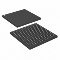
DS33X81+ Maxim Integrated Products, DS33X81+ Datasheet - Page 25

DS33X81+
Manufacturer Part Number
DS33X81+
Description
IC MAPPING ETHERNET 256CSBGA
Manufacturer
Maxim Integrated Products
Datasheet
1.DS33X11.pdf
(375 pages)
Specifications of DS33X81+
Applications
Data Transport
Interface
Parallel/Serial
Voltage - Supply
1.8V, 2.5V, 3.3V
Package / Case
256-CSBGA
Mounting Type
Surface Mount
Lead Free Status / RoHS Status
Lead free / RoHS Compliant
- Current page: 25 of 375
- Download datasheet (3Mb)
Rev: 063008
________________________________________________ DS33X162/X161/X82/X81/X42/X41/X11/W41/W11
SDATA[10]
SDATA[11]
SDATA[12]
SDATA[13]
SDATA[14]
SDATA[15]
REF_CLK
GTX_CLK
SDATA[0]
SDATA[1]
SDATA[2]
SDATA[3]
SDATA[4]
SDATA[5]
SDATA[6]
SDATA[7]
SDATA[8]
SDATA[9]
SDA[10]
SDA[11]
SDA[12]
SBA[0],
SDA[0]
SDA[1]
SDA[2]
SDA[3]
SDA[4]
SDA[5]
SDA[6]
SDA[7]
SDA[8]
SDA[9]
SBA[1]
NAME
MDIO
SDCS
MDC
PACKAGE PINS
B4, B3
G13
R14
F15
C16
B16
B15
C15
A14
C12
A13
B13
D12
C10
B10
B11
C11
B12
256
T13
D9
C9
C3
C2
B2
A2
D3
D4
B5
C5
D5
B6
A3
C6
A5
A4
D4, C4
M10
A11
B11
D11
C11
A10
B10
D10
C10
144
M8
H5
C8
D8
C9
D9
D2
D1
C1
C2
C3
D3
H4
B8
E9
B9
A9
A3
B2
E1
E2
B3
A4
B4
A5
TYPE
IOz
IO
O
O
O
O
I
I
PHY MANAGEMENT BUS
SDRAM CONTROLLER
Reference Clock Input. REF_CLK must be 125MHz for GMII operation.
REF_CLK must be 25MHz for MII DCE operation. REF_CLK must be
50MHz for RMII operation.
GbE Transmit Clock Output (GMII). 125MHz clock output available for
GMII operation. This clock is sourced from the 125MHz REF_CLK input.
Management Data Clock. Clocks management data to and from the PHY.
The clock is derived from SYSCLKI, with a maximum frequency is
1.67MHz.
MII Management Data IO. Data path for control information between the
device and the PHY. Pull to logic high externally through a 1.5 kΩ resistor.
The MDC and MDIO pins are used to write or read up to 32 Control and
Status Registers in PHY Controllers. This port can also be used to initiate
Auto-Negotiation for the PHY.
SDRAM Data Bus Bits 0 through 15. The 16 pins of the SDRAM data
bus are inputs for read operations and outputs for write operations. At all
other times, these pins are high impedance.
SDRAM Address Bus 0 through 12. The 13 pins of the SDRAM address
bus output the row address first, followed by the column address. The row
address is determined by SDA[0] to SDA[12] at the rising edge of clock.
Column address is determined by SDA[0]-SDA[9] and SDA[11] at the
rising edge of the clock. SDA[10] is used as an auto-precharge signal.
SDRAM Bank Select. These 2 bits select 1 of 4 banks for the
read/write/precharge operations.
SDRAM Chip Select.All commands are masked when SDCS is registered
high. SDCS provides for external bank selection on systems with multiple
banks. SDCS is considered part of the command code.
FUNCTION
25 of 375
Related parts for DS33X81+
Image
Part Number
Description
Manufacturer
Datasheet
Request
R

Part Number:
Description:
MAX7528KCWPMaxim Integrated Products [CMOS Dual 8-Bit Buffered Multiplying DACs]
Manufacturer:
Maxim Integrated Products
Datasheet:

Part Number:
Description:
Single +5V, fully integrated, 1.25Gbps laser diode driver.
Manufacturer:
Maxim Integrated Products
Datasheet:

Part Number:
Description:
Single +5V, fully integrated, 155Mbps laser diode driver.
Manufacturer:
Maxim Integrated Products
Datasheet:

Part Number:
Description:
VRD11/VRD10, K8 Rev F 2/3/4-Phase PWM Controllers with Integrated Dual MOSFET Drivers
Manufacturer:
Maxim Integrated Products
Datasheet:

Part Number:
Description:
Highly Integrated Level 2 SMBus Battery Chargers
Manufacturer:
Maxim Integrated Products
Datasheet:

Part Number:
Description:
Current Monitor and Accumulator with Integrated Sense Resistor; ; Temperature Range: -40°C to +85°C
Manufacturer:
Maxim Integrated Products

Part Number:
Description:
TSSOP 14/A�/RS-485 Transceivers with Integrated 100O/120O Termination Resis
Manufacturer:
Maxim Integrated Products

Part Number:
Description:
TSSOP 14/A�/RS-485 Transceivers with Integrated 100O/120O Termination Resis
Manufacturer:
Maxim Integrated Products

Part Number:
Description:
QFN 16/A�/AC-DC and DC-DC Peak-Current-Mode Converters with Integrated Step
Manufacturer:
Maxim Integrated Products

Part Number:
Description:
TDFN/A/65V, 1A, 600KHZ, SYNCHRONOUS STEP-DOWN REGULATOR WITH INTEGRATED SWI
Manufacturer:
Maxim Integrated Products

Part Number:
Description:
Integrated Temperature Controller f
Manufacturer:
Maxim Integrated Products

Part Number:
Description:
SOT23-6/I�/45MHz to 650MHz, Integrated IF VCOs with Differential Output
Manufacturer:
Maxim Integrated Products

Part Number:
Description:
SOT23-6/I�/45MHz to 650MHz, Integrated IF VCOs with Differential Output
Manufacturer:
Maxim Integrated Products

Part Number:
Description:
EVALUATION KIT/2.4GHZ TO 2.5GHZ 802.11G/B RF TRANSCEIVER WITH INTEGRATED PA
Manufacturer:
Maxim Integrated Products

Part Number:
Description:
QFN/E/DUAL PCIE/SATA HIGH SPEED SWITCH WITH INTEGRATED BIAS RESISTOR
Manufacturer:
Maxim Integrated Products
Datasheet:


