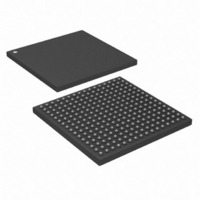
DS33W41+ Maxim Integrated Products, DS33W41+ Datasheet - Page 29

DS33W41+
Manufacturer Part Number
DS33W41+
Description
IC MAPPING ETHERNET 256CSBGA
Manufacturer
Maxim Integrated Products
Datasheet
1.DS33X11.pdf
(375 pages)
Specifications of DS33W41+
Applications
Data Transport
Interface
Parallel/Serial
Voltage - Supply
1.8V, 2.5V, 3.3V
Package / Case
256-CSBGA
Mounting Type
Surface Mount
Lead Free Status / RoHS Status
Lead free / RoHS Compliant
- Current page: 29 of 375
- Download datasheet (3Mb)
Rev: 063008
________________________________________________ DS33X162/X161/X82/X81/X42/X41/X11/W41/W11
SYSCLKI
RVSYNC
VDD3.3
VDD1.8
RVDEN
JTCLK
NAME
JTRST
JTDO
JTMS
JTDI
RST
HIZ
E3, E4,
PACKAGE PINS
E9, F7,
D11,
G12,
H11,
H12,
E10,
E12,
F12,
H16
E16
R13
256
G5,
M8,
T14
M3,
K5,
P4,
G3
E2
D2
C1
F4
E8
B1
A1
K12,
H12,
F11,
M11
144
F10
E12
M2,
M5,
H1,
H6,
H7,
G6,
G7,
F3,
F1,
G4
G3
G2
M7
L1,
F2
H2
H3
—
—
TYPE
Ipu
Ipu
Ipu
Ipu
Oz
I
I
I
I
I
I
I
HARDWARE AND STATUS PINS
Receive Voice Synchronization Input. Receive sync that indicates
frame boundaries present on RVDATA – referenced to RVCLK, frequency
of 8 kHz. This signal is only available on the DS33W41 and DS33W11.
Receive Voice Data Enable: May be used in place of a gapped RVCLK.
If low, RVDATA is valid. If gapped RVCLK is used and this signal is not
used, tie this input low. This signal is only available on the DS33W41 and
DS33W11.
High-Impedance Test Enable (Active Low). This signal puts all digital
output and bi-directional pins in the high impedance state when it is low
and JTRST is low. For normal operation tie high. This is an asynchronous
input.
Reset (Active Low). An active low signal on this pin resets the internal
registers and logic. While this pin is held low, the microprocessor interface
is kept in a high-impedance state. This pin should remain low until power
is stable and then set high for normal operation.
System Clock In: 125MHz, ±100ppm System Clock input.
JTAG Reset (Active Low). JTRST is used to asynchronously reset the
test access port controller. After power-up, a rising edge on JTRST will
reset the test port and cause the device I/O to enter the JTAG DEVICE ID
mode. Pulling JTRST low restores normal device operation. JTRST is
pulled HIGH internally via a 10kΩ resistor operation. If boundary scan is
not used, this pin should be held low.
JTAG Clock. This signal is used to shift data into JTDI on the rising edge
and out of JTDO on the falling edge.
JTAG Data Out. Test instructions and data are clocked out of this pin on
the falling edge of JTCLK. If not used, this pin should be left unconnected.
JTAG Data In. Test instructions and data are clocked into this pin on the
rising edge of JTCLK. This pin has a 10kΩ pullup resistor.
JTAG Mode Select. This pin is sampled on the rising edge of JTCLK and
is used to place the test access port into the various defined IEEE 1149.1
states. This pin has a 10kΩ pullup resistor.
Connect to 3.3V Power Supply
Connect to 1.8V Power Supply
POWER SUPPLIES
JTAG INTERFACE
SYSTEM CLOCKS
FUNCTION
29 of 375
Related parts for DS33W41+
Image
Part Number
Description
Manufacturer
Datasheet
Request
R

Part Number:
Description:
MAX7528KCWPMaxim Integrated Products [CMOS Dual 8-Bit Buffered Multiplying DACs]
Manufacturer:
Maxim Integrated Products
Datasheet:

Part Number:
Description:
Single +5V, fully integrated, 1.25Gbps laser diode driver.
Manufacturer:
Maxim Integrated Products
Datasheet:

Part Number:
Description:
Single +5V, fully integrated, 155Mbps laser diode driver.
Manufacturer:
Maxim Integrated Products
Datasheet:

Part Number:
Description:
VRD11/VRD10, K8 Rev F 2/3/4-Phase PWM Controllers with Integrated Dual MOSFET Drivers
Manufacturer:
Maxim Integrated Products
Datasheet:

Part Number:
Description:
Highly Integrated Level 2 SMBus Battery Chargers
Manufacturer:
Maxim Integrated Products
Datasheet:

Part Number:
Description:
Current Monitor and Accumulator with Integrated Sense Resistor; ; Temperature Range: -40°C to +85°C
Manufacturer:
Maxim Integrated Products

Part Number:
Description:
TSSOP 14/A�/RS-485 Transceivers with Integrated 100O/120O Termination Resis
Manufacturer:
Maxim Integrated Products

Part Number:
Description:
TSSOP 14/A�/RS-485 Transceivers with Integrated 100O/120O Termination Resis
Manufacturer:
Maxim Integrated Products

Part Number:
Description:
QFN 16/A�/AC-DC and DC-DC Peak-Current-Mode Converters with Integrated Step
Manufacturer:
Maxim Integrated Products

Part Number:
Description:
TDFN/A/65V, 1A, 600KHZ, SYNCHRONOUS STEP-DOWN REGULATOR WITH INTEGRATED SWI
Manufacturer:
Maxim Integrated Products

Part Number:
Description:
Integrated Temperature Controller f
Manufacturer:
Maxim Integrated Products

Part Number:
Description:
SOT23-6/I�/45MHz to 650MHz, Integrated IF VCOs with Differential Output
Manufacturer:
Maxim Integrated Products

Part Number:
Description:
SOT23-6/I�/45MHz to 650MHz, Integrated IF VCOs with Differential Output
Manufacturer:
Maxim Integrated Products

Part Number:
Description:
EVALUATION KIT/2.4GHZ TO 2.5GHZ 802.11G/B RF TRANSCEIVER WITH INTEGRATED PA
Manufacturer:
Maxim Integrated Products

Part Number:
Description:
QFN/E/DUAL PCIE/SATA HIGH SPEED SWITCH WITH INTEGRATED BIAS RESISTOR
Manufacturer:
Maxim Integrated Products
Datasheet:


