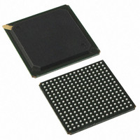
PI7C9X20508GPBNDE Pericom Semiconductor, PI7C9X20508GPBNDE Datasheet - Page 14

PI7C9X20508GPBNDE
Manufacturer Part Number
PI7C9X20508GPBNDE
Description
IC PCIE PACKET SWITCH 256BGA
Manufacturer
Pericom Semiconductor
Series
GreenPacket™r
Specifications of PI7C9X20508GPBNDE
Applications
Data Transport
Interface
Advanced Configuration Power Interface (ACPI)
Package / Case
256-PBGA
Mounting Type
Surface Mount
Lead Free Status / RoHS Status
Lead free / RoHS Compliant
Voltage - Supply
-
Available stocks
Company
Part Number
Manufacturer
Quantity
Price
Company:
Part Number:
PI7C9X20508GPBNDE
Manufacturer:
Pericom
Quantity:
200
3.5 JTAG BOUNDARY SCAN SIGNALS
June 2009 – Revision 1.5
Pericom Semiconductor
Name
TCK
TMS
TDO
TDI
NAME
PORTERR [4:0]
GPIO [7:0]
HIDRV
LODRV
DTX [3:0]
DEQ [3:0]
RXEQCTL [1:0]
RXTERMADJ [1:0]
TXTERMADJ [1:0]
TEST1
TEST2
TEST3
TEST4
TEST5
TEST6
NC
L2, L1, K5,
L6
M2
N1, M6, M5,
P4, P3
T3, R2
T2, R1
N13, P13,
M12, N12,
P12
K4, K3, K2,
J6, J5
M3
P1, N5, N4,
N2
L4
D4
D8
E8
E7
E14
D12, D13,
F3, F12, F13,
H12, H13,
R3, R5
L12
L13
M13
L14
PIN
Pin
TYPE
Type
I/O
O
I
I
I
I
I
I
I
I
I
I
O
I
I
I
Page 14 of 81
Description
Test Clock: Used to clock state information and data into and out of
the chip during boundary scan. When JTAG boundary scan function is
not implemented, this pin should be left open (NC).
Test Mode Select: Used to control the state of the Test Access Port
controller. The pin has internal pull-up. When JTAG boundary scan
function is not implemented, this pin should be pulled low through a
5.1K pull-down resistor.
Test Data Output: When SCAN_EN is high, it is used (in conjunction
with TCK) to shift data out of the Test Access Port (TAP) in a serial bit
stream. When JTAG boundary scan function is not implemented, this
pin should be left open (NC).
Test Data Input: When SCAN_EN is high, it is used (in conjunction
with TCK) to shift data and instructions into the TAP in a serial bit
stream. The pin has internal pull-up.When JTAG boundary scan
function is not implemented, this pin should be left open (NC).
DESCRIPTION
Port PHY Error Status: These pins are used to display the PHY Error
status of the ports. When PORTERR is flashing (alternating high and
low signals), it indicates that a PHY error is detected When it is low,
no PHY error is detected. PORTERR [x] is correspondent to Port x,
where x=0,1,2,3,4.
General Purpose Input and Output: These eight general-purpose
pins are programmed as either input-only or bi-directional pins by
writing the GPIO output enable control register.
When SMBus is implemented, GPIO[7:5] act as the SMBus address
pins, which set Bit 2 to 0 of the SMBus address.
High Driver Control: This mode bit is for increasing the nominal
value of the lane’s driver current level. (See Sec. 5.1 for more detailed
descriptions) By default, it is set to ‘0’ without pin strapped.
Low Driver Control: This mode bit is for decreasing the nominal
value of the lane’s driver current level. (See Sec. 5.1 for more detailed
descriptions) By default, it is set to ‘0’ without pin strapped.
Driver Current Level Control: This 4-bit digital word is to control
the driver current level. (See Sec. 5.1 for more detailed descriptions)
By default, they are set to “0000” without pin strapped.
Driver Equalization Level Control: This 4-bit digital word is to
control the driver equalization level. (See Sec. 5.1 for more detailed
descriptions) By default, they are set to “1000” without pin strapped.
Receiver Equalization Level Control: This 2-bit digital word is to
control the receiver equalization level. By default, they are set to “00”
without pin strapped.
Receive Termination Adjustment: A control bus to adjust the receive
termination resistor value. By default, they are set to “00” without pin
strapped.
Transmit Termination Adjustment: A control bus to adjust the
transmit termination resistor value. By default, they are set to “00”
without pin strapped.
Test1: This pin is for internal test purpose. Test1 should be tied to
ground through a pull-down resistor.
Test2/3/4/5: These pins are for internal test purpose. Test2, Test3,
Test4 and Test5 should be tied to 3.3V through a pull-up resistor.
Test6: This pin is for internal test purpose. Test6 should be connected
an (475 ohm +/- 1%) external resistor to Vss.
Not Connected: These pins can be just left open.
5Port-8Lane PCI Express Switch
GreenPacket
PI7C9X20508GP
Datasheet
TM
Family


