PX1011BI-EL1/G,551 NXP Semiconductors, PX1011BI-EL1/G,551 Datasheet - Page 18
PX1011BI-EL1/G,551
Manufacturer Part Number
PX1011BI-EL1/G,551
Description
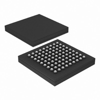
IC PCI-EXPRESS X1 PHY 81-LFBGA
Manufacturer
NXP Semiconductors
Specifications of PX1011BI-EL1/G,551
Package / Case
81-LFBGA
Applications
PCI Express MAX to PCI Express PHY
Interface
JTAG
Voltage - Supply
1.2 V
Mounting Type
Surface Mount
Input Voltage Range (max)
0.31 V
Maximum Operating Temperature
+ 85 C
Maximum Power Dissipation
300 mW
Minimum Operating Temperature
- 40 C
Mounting Style
SMD/SMT
Operating Supply Voltage
1.2 V
Supply Current (max)
28 mA
Lead Free Status / RoHS Status
Lead free / RoHS Compliant
Lead Free Status / RoHS Status
Lead free / RoHS Compliant, Lead free / RoHS Compliant
Other names
935282114551
PX1011BI-EL1/G-S
PX1011BI-EL1/G-S
PX1011BI-EL1/G-S
PX1011BI-EL1/G-S
Available stocks
Company
Part Number
Manufacturer
Quantity
Price
Company:

Part Number:
PX1011BI-EL1/G,551
Manufacturer:
NXP Semiconductors
Quantity:
10 000


NXP Semiconductors
PX1011B_4
Product data sheet
8.12 Setting negative disparity
8.13 JTAG boundary scan interface
To set the running disparity to negative, the MAC asserts TXCOMP for one clock cycle
that matches with the data that is to be transmitted with negative disparity.
Joint Test Action Group (JTAG) or IEEE 1149.1 is a standard, specifying how to control
and monitor the pins of compliant devices on a printed-circuit board. This standard is
commonly known as ‘JTAG Boundary Scan’.
This standard defines a 5-pin serial protocol for accessing and controlling the signal levels
on the pins of a digital circuit, and has some extensions for testing the internal circuitry on
the chip itself, which is beyond the scope of this data sheet.
Access to the JTAG interface is provided to the customer for the sole purpose of using
boundary scan for interconnect test verification between other compliant devices that may
reside on the board. Using JTAG for purposes other than boundary scan may produce
undesired effects.
The JTAG interface is a 3.3 V CMOS signaling. JTAG TRST_N must be asserted LOW for
normal device operation. If JTAG is not planned to be used, it is recommended to
pull down TRST_N to V
Fig 16. Setting negative disparity
TXDATA[7:0]
TX_P, TX_N
TXCOMP
TXCLK
data
valid data
Rev. 04 — 4 September 2009
SS
.
K28.5
K28.5
PCI Express stand-alone X1 PHY
K28.5
K28.5
byte transmitted
with negative disparity
K28.5
K28.5
PX1011B
© NXP B.V. 2009. All rights reserved.
002aac177
18 of 30
Related parts for PX1011BI-EL1/G,551
Image
Part Number
Description
Manufacturer
Datasheet
Request
R

Part Number:
Description:
IC PCI-EXPRESS X1 PHY 81-LFBGA
Manufacturer:
NXP Semiconductors
Datasheet:

Part Number:
Description:
Telecom Line Management ICs PCI EXPRESS STAND ALONE X1 PHY
Manufacturer:
NXP Semiconductors
Part Number:
Description:
Telecom Line Management ICs PCI EXPRESS STAND ALONE X1 PHY
Manufacturer:
NXP Semiconductors
Part Number:
Description:
IC PCI-EXPRESS X1 PHY 81LFBGA
Manufacturer:
NXP Semiconductors
Datasheet:
Part Number:
Description:
Manufacturer:
NXP Semiconductors
Datasheet:
Part Number:
Description:
NXP Semiconductors designed the LPC2420/2460 microcontroller around a 16-bit/32-bitARM7TDMI-S CPU core with real-time debug interfaces that include both JTAG andembedded trace
Manufacturer:
NXP Semiconductors
Datasheet:

Part Number:
Description:
NXP Semiconductors designed the LPC2458 microcontroller around a 16-bit/32-bitARM7TDMI-S CPU core with real-time debug interfaces that include both JTAG andembedded trace
Manufacturer:
NXP Semiconductors
Datasheet:
Part Number:
Description:
NXP Semiconductors designed the LPC2468 microcontroller around a 16-bit/32-bitARM7TDMI-S CPU core with real-time debug interfaces that include both JTAG andembedded trace
Manufacturer:
NXP Semiconductors
Datasheet:
Part Number:
Description:
NXP Semiconductors designed the LPC2470 microcontroller, powered by theARM7TDMI-S core, to be a highly integrated microcontroller for a wide range ofapplications that require advanced communications and high quality graphic displays
Manufacturer:
NXP Semiconductors
Datasheet:
Part Number:
Description:
NXP Semiconductors designed the LPC2478 microcontroller, powered by theARM7TDMI-S core, to be a highly integrated microcontroller for a wide range ofapplications that require advanced communications and high quality graphic displays
Manufacturer:
NXP Semiconductors
Datasheet:
Part Number:
Description:
The Philips Semiconductors XA (eXtended Architecture) family of 16-bit single-chip microcontrollers is powerful enough to easily handle the requirements of high performance embedded applications, yet inexpensive enough to compete in the market for hi
Manufacturer:
NXP Semiconductors
Datasheet:
Part Number:
Description:
The XA-S3 device is a member of Philips Semiconductors? XA(eXtended Architecture) family of high performance 16-bitsingle-chip microcontrollers
Manufacturer:
NXP Semiconductors
Datasheet:

Part Number:
Description:
The NXP BlueStreak LH75401/LH75411 family consists of two low-cost 16/32-bit System-on-Chip (SoC) devices
Manufacturer:
NXP Semiconductors
Datasheet:
Part Number:
Description:
The NXP LPC3130/3131 combine an 180 MHz ARM926EJ-S CPU core, high-speed USB2
Manufacturer:
NXP Semiconductors
Datasheet: