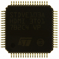
STDVE103ABTR STMicroelectronics, STDVE103ABTR Datasheet - Page 17

STDVE103ABTR
Manufacturer Part Number
STDVE103ABTR
Description
IC EQUALIZER TMDS/HDMI 64-TQFP
Manufacturer
STMicroelectronics
Datasheet
1.STDVE103ABTR.pdf
(44 pages)
Specifications of STDVE103ABTR
Applications
TV
Interface
I²C
Voltage - Supply
3.3V, 5V
Package / Case
64-TQFP, 64-VQFP
Mounting Type
Surface Mount
Lead Free Status / RoHS Status
Lead free / RoHS Compliant
Other names
497-8384-2
Available stocks
Company
Part Number
Manufacturer
Quantity
Price
Company:
Part Number:
STDVE103ABTR
Manufacturer:
TI
Quantity:
9 925
Company:
Part Number:
STDVE103ABTR
Manufacturer:
STMicroelectronics
Quantity:
10 000
Part Number:
STDVE103ABTR
Manufacturer:
ST
Quantity:
20 000
STDVE103A
4.7
4.8
Bias
The bandgap reference voltage over the external R
bias reference current. This current and its factors (achieved by employing highly accurate
and well matched current mirror circuit topologies) are generated on-chip and used by
several internal modules. The 10 mA current used by the transmitter block is also generated
using this reference current. It is important to ensure that the R
tolerance range of its typical value.
Table 5.
The output voltage swing depends on 3 components: supply voltage (V
resistor (R
termination resistor can vary from 50
The voltage on the output is given by:
The variation on I
the HDMI specification under all conditions.
This is achieved when:
with typical value centered at 500 mV.
Timing between HPD and DDC
It is important to ensure that the I
complete.
As soon as the discovery is finished by the HPD detection, the configuration data is
exchanged between a source and sink through the I
DDC interface is ready for communication as soon as the power supply to the chip is
present and stable. When the desired port is enabled and the chip is out of shutdown mode,
the I
Thus, as soon as the HPD detection sequence is complete, the DDC interface can be
readily used. There is no delay between the HPD detection and I
ready.
Bandgap voltage
Parameter
2
C DDC lines can be used for communication.
T
) and current drive (I
Bias parameter
drive
must be controlled to ensure that the voltage on HDMI output is within
Min
-
Doc ID 14911 Rev 4
drive
2
400mV I
C DDC interface is ready by the time the HPD detection is
). The supply voltage can vary from 3.3 V
V
Ω ±
supply
≤
10%.
drive
–
Typ
1.2
I
drive
×
R
T
×
≤
EXT
600mV
2
R
C DDC interface. The STDVE003’s
T
reference resistor sets the internal
Max
EXT
-
2
C DDC interface to be
value is within the ±1%
Functional description
supply)
, termination
±
5%,
Unit
V
17/44


