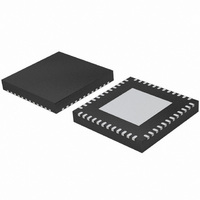
PTN3360BBS,518 NXP Semiconductors, PTN3360BBS,518 Datasheet - Page 14

PTN3360BBS,518
Manufacturer Part Number
PTN3360BBS,518
Description
IC DVI/HDMI LEVEL SHIFT 48-HVQFN
Manufacturer
NXP Semiconductors
Type
Level Shifterr
Datasheet
1.PTN3360BBS518.pdf
(22 pages)
Specifications of PTN3360BBS,518
Package / Case
48-VQFN Exposed Pad, 48-HVQFN, 48-SQFN, 48-DHVQFN
Applications
Set-Top Boxes, Video Players
Interface
3-Wire Serial
Voltage - Supply
3 V ~ 3.6 V
Mounting Type
Surface Mount
Maximum Operating Temperature
+ 85 C
Minimum Operating Temperature
- 40 C
Mounting Style
SMD/SMT
Lead Free Status / RoHS Status
Lead free / RoHS Compliant
Lead Free Status / RoHS Status
Lead free / RoHS Compliant, Lead free / RoHS Compliant
Other names
568-4777-2
NXP Semiconductors
Table 8.
[1]
[2]
[3]
[4]
[5]
[6]
[7]
Table 9.
[1]
[2]
[3]
[4]
[5]
PTN3360B_2
Product data sheet
Symbol
V
V
I
t
t
t
t
Symbol
V
V
I
V
V
t
t
R
OZ
r
f
sk
jit
LI
PD
t
V
OH(se)
OL(se)
IH
IL
OH
OL
pd
O(se)
V
The open-drain output pulls down from V
Swing down from TMDS termination voltage (3.3 V
Maximum rise/fall time at 2.5 Gbit/s = 400 ps. 360 ps = 400 ps
This differential skew budget is in addition to the skew presented between IN_D+ and IN_D paired input pins.
This lane-to-lane skew budget is in addition to skew between differential input pairs.
Jitter budget for differential signals as they pass through the level shifter.
Low-speed input changes state on cable plug/unplug.
Measured with HPD_SINK at V
Time from HPD_SINK changing state to HPD_SOURCE changing state. Includes HPD_SOURCE rise/fall time.
Time required to transition from V
Guarantees HPD_SINK is LOW when no display is plugged in.
TT
is the DC termination voltage in the HDMI or DVI sink. V
Differential output characteristics for OUT_Dx signals
HPD characteristics
Parameter
single-ended HIGH-level
output voltage
single-ended LOW-level
output voltage
single-ended output
voltage variation
OFF-state output current
rise time
fall time
skew time
jitter time
Parameter
HIGH-level input voltage
LOW-level input voltage
input leakage current
HIGH-level output voltage
LOW-level output voltage
propagation delay
transition time
pull-down resistance
9.2 Differential outputs
9.3 HPD_SINK input, HPD_SOURCE output
The level shifter’s differential outputs are designed to meet HDMI version 1.3 and
DVI version 1.0 specifications.
IH
OH
maximum and V
to V
Conditions
logic 1 and logic 0 state applied
respectively to differential inputs
IN_Dn; R
see
single-ended
20 % to 80 %
80 % to 20 %
intra-pair
inter-pair
jitter contribution
TT
OL
.
Conditions
HPD_SINK
HPD_SINK
HPD_SINK
HPD_SOURCE
HPD_SOURCE
from HPD_SINK to HPD_SOURCE;
50 % to 50 %
HPD_SOURCE rise/fall; 10 % to 90 %
HPD_SINK input pull-down resistor
or from V
Table 5
IL
ref(ext)
Rev. 02 — 8 October 2009
minimum.
OL
10 %).
to V
connected;
OH
TT
.
is nominally 3.3 V.
10 %.
Enhanced performance HDMI/DVI level shifter
[1]
[2]
[3]
[4]
[4]
[5]
[6]
[7]
Min
V
V
400
-
75
75
-
-
-
TT
TT
[1]
[2]
[3]
[4]
[5]
0.01 V
0.60 V
Min
2.0
0
-
2.5
0
-
1
100
Typ
500
-
-
-
-
-
-
TT
TT
Typ
5.0
-
-
-
-
-
-
200
0.50 V
PTN3360B
© NXP B.V. 2009. All rights reserved.
Max
V
600
10
160
160
10
250
7.4
TT
TT
Max
5.3
0.8
10
V
0.2
200
20
300
+ 0.01 V
DD
0.40 V
14 of 22
Unit
V
V
V
V
ns
ns
k
Unit
mV
ps
ps
ps
ps
ps
A
A


