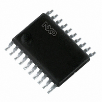
PCA9545BPW,118 NXP Semiconductors, PCA9545BPW,118 Datasheet - Page 6

PCA9545BPW,118
Manufacturer Part Number
PCA9545BPW,118
Description
IC I2C SWITCH 4CH 20-TSSOP
Manufacturer
NXP Semiconductors
Datasheet
1.PCA9545BPW118.pdf
(28 pages)
Specifications of PCA9545BPW,118
Package / Case
20-TSSOP
Applications
4-Channel I²C Switcher
Interface
I²C
Voltage - Supply
2.3 V ~ 3.6 V, 4.5 V ~ 5.5 V
Mounting Type
Surface Mount
Product
Multiplexer
Number Of Lines (input / Output)
4.0 / 1.0
Propagation Delay Time
0.3 ns at 2.3 V to 5.5 V
Supply Voltage (max)
5.5 V
Supply Voltage (min)
2.3 V
Maximum Operating Temperature
+ 85 C
Minimum Operating Temperature
- 40 C
Mounting Style
SMD/SMT
Number Of Input Lines
4.0
Number Of Output Lines
1.0
Logical Function
I2C Multiplexer
Configuration
1 x 4:1
Number Of Inputs
4
Number Of Outputs
1
Operating Supply Voltage (typ)
2.5/3.3/5V
Operating Supply Voltage (min)
2.3V
Operating Supply Voltage (max)
5.5V
Power Dissipation
400mW
Operating Temp Range
-40C to 85C
Operating Temperature Classification
Industrial
Mounting
Surface Mount
Pin Count
20
Package Type
TSSOP
Lead Free Status / RoHS Status
Lead free / RoHS Compliant
Lead Free Status / RoHS Status
Lead free / RoHS Compliant, Lead free / RoHS Compliant
Other names
568-4246-2
935283307118
PCA9545BPW-T
935283307118
PCA9545BPW-T
NXP Semiconductors
6. Functional description
PCA9545A_45B_45C_7
Product data sheet
6.1 Device address
Refer to
Following a START condition, the bus master must output the address of the slave it is
accessing. The address of the PCA9545A is shown in
internal pull-up resistors are incorporated on the hardware selectable address pins and
they must be pulled HIGH or LOW.
The last bit of the slave address defines the operation to be performed. When set to
logic 1, a read is selected while a logic 0 selects a write operation.
The PCA9545BPW and PCA9545CPW are alternate address versions if needed for larger
systems or to resolve conflicts. The data sheet will reference the PCA9545A, but the
PCA9545B and PCA9545C function identically except for the slave address.
Fig 5.
Fig 6.
1
Figure 1 “Block diagram of
Slave address PCA9545A
Slave address PCA9545B
1
fixed
0
1
Rev. 07 — 19 June 2009
0
selectable
hardware
A1
1
A0 R/W
002aab835
4-channel I
1
PCA9545A/45B/45C”.
fixed
1
0
2
C-bus switch with interrupt logic and reset
0
Fig 7.
PCA9545A/45B/45C
selectable
hardware
A1
1
A0 R/W
002aab169
Slave address PCA9545C
Figure
0
fixed
1
5. To conserve power, no
1
0
selectable
© NXP B.V. 2009. All rights reserved.
hardware
A1
002aab836
A0 R/W
6 of 28


