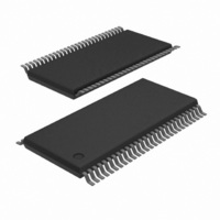
PCA9506DGG,518 NXP Semiconductors, PCA9506DGG,518 Datasheet - Page 27

PCA9506DGG,518
Manufacturer Part Number
PCA9506DGG,518
Description
IC I/O EXPANDER I2C 40B 56TSSOP
Manufacturer
NXP Semiconductors
Specifications of PCA9506DGG,518
Package / Case
56-TSSOP
Interface
I²C
Number Of I /o
40
Interrupt Output
Yes
Frequency - Clock
400kHz
Voltage - Supply
2.3 V ~ 5.5 V
Operating Temperature
-40°C ~ 85°C
Mounting Type
Surface Mount
Includes
POR
Logic Family
PCA9506
Number Of Lines (input / Output)
40.0 / 40.0
Operating Supply Voltage
2.3 V to 5.5 V
Power Dissipation
500 mW
Operating Temperature Range
- 40 C to + 85 C
Input Voltage
5.5 V
Logic Type
I/O Expander
Maximum Clock Frequency
400 KHz
Mounting Style
SMD/SMT
Number Of Input Lines
40.0
Number Of Output Lines
40.0
Output Current
50 mA
Output Voltage
5.5 V
Operating Temperature (min)
-40C
Operating Temperature Classification
Industrial
Operating Temperature (max)
85C
Package Type
TSSOP
Rad Hardened
No
Lead Free Status / RoHS Status
Lead free / RoHS Compliant
Lead Free Status / RoHS Status
Lead free / RoHS Compliant, Lead free / RoHS Compliant
Other names
935280798518
PCA9506DGG-T
PCA9506DGG-T
PCA9506DGG-T
PCA9506DGG-T
Philips Semiconductors
9397 750 14939
Product data sheet
16.4 Manual soldering
16.5 Package related soldering information
During placement and before soldering, the package must be fixed with a droplet of
adhesive. The adhesive can be applied by screen printing, pin transfer or syringe
dispensing. The package can be soldered after the adhesive is cured.
Typical dwell time of the leads in the wave ranges from 3 seconds to 4 seconds at 250 C
or 265 C, depending on solder material applied, SnPb or Pb-free respectively.
A mildly-activated flux will eliminate the need for removal of corrosive residues in most
applications.
Fix the component by first soldering two diagonally-opposite end leads. Use a low voltage
(24 V or less) soldering iron applied to the flat part of the lead. Contact time must be
limited to 10 seconds at up to 300 C.
When using a dedicated tool, all other leads can be soldered in one operation within
2 seconds to 5 seconds between 270 C and 320 C.
Table 12:
[1]
Package
BGA, HTSSON..T
SSOP..T
DHVQFN, HBCC, HBGA, HLQFP, HSO, HSOP,
HSQFP, HSSON, HTQFP, HTSSOP, HVQFN,
HVSON, SMS
PLCC
LQFP, QFP, TQFP
SSOP, TSSOP, VSO, VSSOP
CWQCCN..L
•
•
•
Use a double-wave soldering method comprising a turbulent wave with high upward
pressure followed by a smooth laminar wave.
For packages with leads on two sides and a pitch (e):
– larger than or equal to 1.27 mm, the footprint longitudinal axis is preferred to be
– smaller than 1.27 mm, the footprint longitudinal axis must be parallel to the
The footprint must incorporate solder thieves at the downstream end.
For packages with leads on four sides, the footprint must be placed at a 45 angle to
the transport direction of the printed-circuit board. The footprint must incorporate
solder thieves downstream and at the side corners.
For more detailed information on the BGA packages refer to the (LF)BGA Application Note (AN01026);
order a copy from your Philips Semiconductors sales office.
[5]
parallel to the transport direction of the printed-circuit board;
transport direction of the printed-circuit board.
, SO, SOJ
[3]
[1]
, TFBGA, VFBGA, XSON
Suitability of surface mount IC packages for wave and reflow soldering methods
[8]
, PMFP
[3]
, LBGA, LFBGA, SQFP,
[9]
Rev. 01 — 14 February 2006
, WQCCN..L
[8]
40-bit I
2
Soldering method
Wave
not suitable
not suitable
suitable
not recommended
not recommended
not suitable
C-bus I/O port with RESET, OE, and INT
[4]
© Koninklijke Philips Electronics N.V. 2006. All rights reserved.
[5] [6]
[7]
PCA9506
Reflow
suitable
suitable
suitable
suitable
suitable
not suitable
[2]
27 of 30


