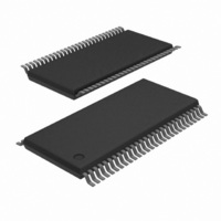
PCA9506DGG,518 NXP Semiconductors, PCA9506DGG,518 Datasheet - Page 21

PCA9506DGG,518
Manufacturer Part Number
PCA9506DGG,518
Description
IC I/O EXPANDER I2C 40B 56TSSOP
Manufacturer
NXP Semiconductors
Specifications of PCA9506DGG,518
Package / Case
56-TSSOP
Interface
I²C
Number Of I /o
40
Interrupt Output
Yes
Frequency - Clock
400kHz
Voltage - Supply
2.3 V ~ 5.5 V
Operating Temperature
-40°C ~ 85°C
Mounting Type
Surface Mount
Includes
POR
Logic Family
PCA9506
Number Of Lines (input / Output)
40.0 / 40.0
Operating Supply Voltage
2.3 V to 5.5 V
Power Dissipation
500 mW
Operating Temperature Range
- 40 C to + 85 C
Input Voltage
5.5 V
Logic Type
I/O Expander
Maximum Clock Frequency
400 KHz
Mounting Style
SMD/SMT
Number Of Input Lines
40.0
Number Of Output Lines
40.0
Output Current
50 mA
Output Voltage
5.5 V
Operating Temperature (min)
-40C
Operating Temperature Classification
Industrial
Operating Temperature (max)
85C
Package Type
TSSOP
Rad Hardened
No
Lead Free Status / RoHS Status
Lead free / RoHS Compliant
Lead Free Status / RoHS Status
Lead free / RoHS Compliant, Lead free / RoHS Compliant
Other names
935280798518
PCA9506DGG-T
PCA9506DGG-T
PCA9506DGG-T
PCA9506DGG-T
Philips Semiconductors
12. Dynamic characteristics
Table 11:
[1]
[2]
[3]
[4]
9397 750 14939
Product data sheet
Symbol
f
t
t
t
t
t
t
t
t
t
t
t
t
t
Port timing
t
t
t
t
t
Interrupt timing
t
t
Reset
t
t
t
SCL
BUF
HD;STA
SU;STA
SU;STO
HD;DAT
VD;ACK
VD;DAT
SU;DAT
LOW
HIGH
f
r
SP
en
dis
v(Q)
su(D)
h(D)
v(INT_N)
rst(INT_N)
w(rst)
rec(rst)
rst
Minimum SCL clock frequency is limited by the bus time-out feature, which resets the serial bus interface if either SDA or SCL is held
LOW for a minimum of 25 ms. Disable bus time-out feature for DC operation.
t
t
A master device must internally provide a hold time of at least 300 ns for the SDA signal (refer to the V
bridge the undefined region SCL’s falling edge.
VD;ACK
VD;DAT
= minimum time for SDA data out to be valid following SCL LOW.
= time for Acknowledgement signal from SCL LOW to SDA (out) LOW.
Parameter
SCL clock frequency
bus free time between a STOP and
START condition
hold time (repeated) START
condition
set-up time for a repeated START
condition
set-up time for STOP condition
data hold time
data valid acknowledge time
data valid time
data set-up time
LOW period of the SCL clock
HIGH period of the SCL clock
fall time of both SDA and SCL
signals
rise time of both SDA and SCL
signals
pulse width of spikes that must be
suppressed by the input filter
enable time
disable time
data output valid time
data input setup time
data input hold time
valid time on pin INT_N
reset time on pin INT_N
reset pulse width
reset recovery time
reset time
Dynamic characteristics
[3]
[2]
Rev. 01 — 14 February 2006
Conditions
output
output
[4] [5]
[4] [5]
[1]
[7]
40-bit I
Standard mode
Min
250
100
100
4.7
4.0
4.7
4.0
0.1
0.1
4.7
4.0
0.5
0
0
4
0
-
-
-
-
-
-
-
-
2
I
2
C-bus I/O port with RESET, OE, and INT
C-bus
1000
Max
3.45
3.45
100
300
250
50
80
40
4
4
-
-
-
-
-
-
-
-
-
-
-
-
-
© Koninklijke Philips Electronics N.V. 2006. All rights reserved.
20 + 0.1C
20 + 0.1C
Fast mode I
IL
Min
100
100
100
1.3
0.6
0.6
0.6
0.1
0.1
1.3
0.6
0.5
of the SCL signal) in order to
0
0
4
0
-
-
-
-
-
-
b
b
PCA9506
[6]
[6]
2
C-bus
Max
400
300
300
250
0.9
0.9
50
80
40
4
4
-
-
-
-
-
-
-
-
-
-
-
-
-
21 of 30
Unit
kHz
ns
ns
ns
ns
ns
ns
ns
ns
ns
ns
ns
ns
s
s
s
s
s
s
s
s
s
s
s


