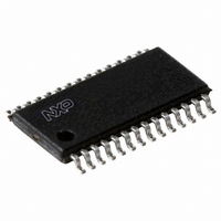
PCA9575PW2,118 NXP Semiconductors, PCA9575PW2,118 Datasheet - Page 8

PCA9575PW2,118
Manufacturer Part Number
PCA9575PW2,118
Description
IC I2C/SMBUS 16BIT GPIO 28-TSSOP
Manufacturer
NXP Semiconductors
Series
-r
Datasheet
1.PCA9575HF118.pdf
(38 pages)
Specifications of PCA9575PW2,118
Interface
I²C, SMBus
Number Of I /o
16
Interrupt Output
Yes
Frequency - Clock
400kHz
Voltage - Supply
1.1 V ~ 3.6 V
Operating Temperature
-40°C ~ 85°C
Mounting Type
Surface Mount
Package / Case
28-TSSOP
Includes
POR
Description/function
16-bit I2C-bus and SMBus
Maximum Operating Temperature
+ 85 C
Minimum Operating Temperature
- 40 C
Mounting Style
SMD/SMT
Supply Voltage (max)
3.6 V
Supply Voltage (min)
1.1 V
Lead Free Status / RoHS Status
Lead free / RoHS Compliant
Other names
935286414118
NXP Semiconductors
7. Functional description
PCA9575_3
Product data sheet
7.1 I/O ports
7.2 Device address
The 16 I/O ports are organized as two banks of 8 ports each. The system master can
enable the I/Os as either inputs or outputs by writing to the I/O configuration register bits.
The data for each input or output is kept in the corresponding Input or Output register. The
polarity of the read register can be inverted with the Polarity Inversion register. Either a
bus-hold function or pull-up/pull-down feature can be selected by programming
corresponding registers. A bus-hold provides a valid logic level when the I/O bus is not
actively driven. It consists of a pair of buffers, one being weak (low drive-strength), that
latch the input at the last driven value. This prevents the input from floating while it is being
driven by a 3-state output. Latching the last valid logic state of input prevents it from
settling at a midpoint between V
driver can easily override the logic level set by the bus-keeper.
When bus-hold feature is not selected, the I/O ports can be configured to have pull-up or
pull-down by programming the pull-up/pull-down configuration register.
Following a START condition, the bus master must send the address of the slave it is
accessing and the operation it wants to perform (read or write). Address configuration for
the device depends on the package type chosen. The device offered in a 24-pin package
will have a fixed slave address for the PCA9575 as shown in
The last bit of the first byte defines the operation to be performed. When set to logic 1 a
read is selected, while logic 0 selects a write operation.
The slave address for the 28-pin version of the PCA9575 is shown in
Fig 6.
Fig 7.
PCA9575 device address for 24-pin version
PCA9575 device address for 28-pin version
Rev. 03 — 9 November 2009
16-bit I
0
0
2
DD
C-bus and SMBus, level translating, low voltage GPIO
fixed
and ground that in turn consumes power. An active bus
1
1
slave address
slave address
0
0
fixed
hardware selectable
A3
0
A2
0
A1
0
002aad567
A0 R/W
002aad583
0
R/W
Figure
6.
Figure
PCA9575
© NXP B.V. 2009. All rights reserved.
7.
8 of 38


