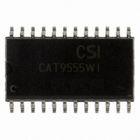
CAT9555WI-T1 ON Semiconductor, CAT9555WI-T1 Datasheet - Page 7

CAT9555WI-T1
Manufacturer Part Number
CAT9555WI-T1
Description
IC I/O EXPANDER I2C 16B 24SOIC
Manufacturer
ON Semiconductor
Datasheet
1.CAT9555WI-T1.pdf
(18 pages)
Specifications of CAT9555WI-T1
Interface
I²C, Serial, SMBus
Number Of I /o
16
Interrupt Output
Yes
Frequency - Clock
400kHz
Voltage - Supply
2.3 V ~ 5.5 V
Operating Temperature
-40°C ~ 85°C
Mounting Type
Surface Mount
Package / Case
24-SOIC (7.5mm Width)
Includes
POR
Lead Free Status / RoHS Status
Lead free / RoHS Compliant
Other names
9555WI-T2
CAT9555WI-T1TR
CAT9555WI-T2
CAT9555WI-T2TR
CAT9555WI-T2TR
CAT9555WI-T1TR
CAT9555WI-T2
CAT9555WI-T2TR
CAT9555WI-T2TR
Available stocks
Company
Part Number
Manufacturer
Quantity
Price
PIN DESCRIPTION
SCL: Serial Clock
The serial clock input clocks all data transferred into
or out of the device. The SCL line requires a pull-up
resistor if it is driven by an open drain output.
SDA: Serial Data/Address
The bidirectional serial data/address pin is used to
transfer all data into and out of the device. The SDA
pin is an open drain output and can be wire-ORed
with other open drain or open collector outputs. A pull-
up resistor must be connected from SDA line to V
The value of the pull-up resistor, R
based on minimum and maximum values from Figure
2 and Figure 3 (see Note).
Note: According to the Fast Mode I²C bus specification, for bus capacitance up to 200pF, the pull up device can
be a resistor. For bus loads between 200pF and 400pF, the pull-up device can be a current source (Imax = 3mA)
or a switched resistor circuit.
© 2010 SCILLC. All rights reserved
Characteristics subject to change without notice
Figure 2. Minimum R
2.5
1.5
0.5
2
1
0
2
2.4 2.8 3.2 3.6
I OL = 3mA @ V OLmax
Supply Voltage
V CC (V)
P
as a Function of
4
P
4.4 4.8 5.2 5.6
, can be calculated
CC
.
7
A0, A1, A2: Device Address Inputs
These inputs are used for extended addressing
capability. The A0, A1, A2 pins should be hardwired to
V
may be addressed on a single bus system. The levels
on these inputs are compared with corresponding bits,
A2, A1, A0, from the slave address byte.
I/O
Any of these pins may be configured as input or
output. The simplified schematic of I/O
shown in Figure 4. When an I/O is configured as an
input, the Q1 and Q2 output transistors are off
creating a high impedance input with a weak pull-up
resistor (typical 100kΩ). If the I/O pin is configured as
an output, the push-pull output stage is enabled. Care
should be taken if an external voltage is applied to an
I/O pin configured as an output due to the low
impedance paths that exist between the pin and either
V
CC
CC
0.0
or V
or V
to I/O
8.00
7.00
6.00
5.00
4.00
3.00
2.00
1.00
0.00
Figure 3. Maximum R
SS
SS
.
. When hardwired, up to eight CAT9555s
0.7
50
Fast Mode I²C Bus / tr max - 300ns
, I/O
100
1.0
Bus Capacitance
to I/O
150
C BUS (pF)
1.7
200
: Input / Output Ports
P
250
Value versus
300
Doc. No. MD-9003, Rev. J
350
0
to I/O
CAT9555
400
7
is


